Photodiode
A photodiode is a semiconductor device that converts light into an electrical current. The current is generated when photons are absorbed in the photodiode. Photodiodes may contain optical filters, built-in lenses, and may have large or small surface areas. Photodiodes usually have a slower response time as their surface area increases. The common, traditional solar cell used to generate electric solar power is a large area photodiode.
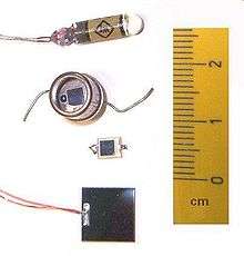
 One Ge (top) and three Si (bottom) photodiodes | |
| Type | Passive |
|---|---|
| Working principle | Converts light into current |
| Pin configuration | anode and cathode |
| Electronic symbol | |
 | |
Photodiodes are similar to regular semiconductor diodes except that they may be either exposed (to detect vacuum UV or X-rays) or packaged with a window or optical fiber connection to allow light to reach the sensitive part of the device. Many diodes designed for use specially as a photodiode use a PIN junction rather than a p–n junction, to increase the speed of response. A photodiode is designed to operate in reverse bias.[1]
Principle of operation
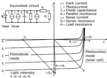
A photodiode is a PIN structure or p–n junction. When a photon of sufficient energy strikes the diode, it creates an electron–hole pair. This mechanism is also known as the inner photoelectric effect. If the absorption occurs in the junction's depletion region, or one diffusion length away from it, these carriers are swept from the junction by the built-in electric field of the depletion region. Thus holes move toward the anode, and electrons toward the cathode, and a photocurrent is produced. The total current through the photodiode is the sum of the dark current (current that is generated in the absence of light) and the photocurrent, so the dark current must be minimized to maximize the sensitivity of the device.[2]
To first order, for a given spectral distribution, the photocurrent is linearly proportional to the irradiance.[3]
Photovoltaic mode

In photovoltaic mode (zero bias), photocurrent flows out of the anode through a short circuit to the cathode. If the circuit is opened or has a load impedance, restricting the photocurrent out of the device, a voltage builds up in the direction that forward biases the diode, that is, anode positive with respect to cathode. If the circuit is shorted or the impedance is low, a forward current will consume all or some of the photocurrent. This mode exploits the photovoltaic effect, which is the basis for solar cells – a traditional solar cell is just a large area photodiode. For optimum power output, the photovoltaic cell will be operated at a voltage that causes only a small forward current compared to the photocurrent.[3]
Photoconductive mode
In photoconductive mode the diode is reverse biased, that is, with the cathode driven positive with respect to the anode. This reduces the response time because the additional reverse bias increases the width of the depletion layer, which decreases the junction's capacitance and increases the region with an electric field that will cause electrons to be quickly collected. The reverse bias also creates dark current without much change in the photocurrent.
Although this mode is faster, the photoconductive mode can exhibit more electronic noise due to dark current or avalanche effects.[4] The leakage current of a good PIN diode is so low (<1 nA) that the Johnson–Nyquist noise of the load resistance in a typical circuit often dominates.
Related devices
Avalanche photodiodes are photodiodes with structure optimized for operating with high reverse bias, approaching the reverse breakdown voltage. This allows each photo-generated carrier to be multiplied by avalanche breakdown, resulting in internal gain within the photodiode, which increases the effective responsivity of the device.

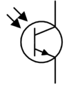
A phototransistor is a light-sensitive transistor. A common type of phototransistor, the bipolar phototransistor, is in essence a bipolar transistor encased in a transparent case so that light can reach the base–collector junction. It was invented by Dr. John N. Shive (more famous for his wave machine) at Bell Labs in 1948[5]:205 but it was not announced until 1950.[6] The electrons that are generated by photons in the base–collector junction are injected into the base, and this photodiode current is amplified by the transistor's current gain β (or hfe). If the base and collector leads are used and the emitter is left unconnected, the phototransistor becomes a photodiode. While phototransistors have a higher responsivity for light they are not able to detect low levels of light any better than photodiodes. Phototransistors also have significantly longer response times. Another type of phototransistor, the field-effect phototransistor (also known as photoFET), is a light-sensitive field-effect transistor. Unlike photobipolar transistors, photoFETs control drain-source current by creating a gate voltage.
A solaristor is a two-terminal gate-less phototransistor. A compact class of two-terminal phototransistors or solaristors have been demonstrated in 2018 by ICN2 researchers. The novel concept is a two-in-one power source plus transistor device that runs on solar energy by exploiting a memresistive effect in the flow of photogenerated carriers.[7]
Materials
The material used to make a photodiode is critical to defining its properties, because only photons with sufficient energy to excite electrons across the material's bandgap will produce significant photocurrents.
Materials commonly used to produce photodiodes are listed in the table below.[8]
| Material | Electromagnetic spectrum wavelength range (nm) |
|---|---|
| Silicon | 190–1100 |
| Germanium | 400–1700 |
| Indium gallium arsenide | 800–2600 |
| Lead(II) sulfide | <1000–3500 |
| Mercury cadmium telluride | 400–14000 |
Because of their greater bandgap, silicon-based photodiodes generate less noise than germanium-based photodiodes.
Binary materials such as MoS2 and graphene emerged as new materials for the production of photodiodes.[9]
Unwanted and wanted photodiode effects
Any p–n junction, if illuminated, is potentially a photodiode. Semiconductor devices such as diodes, transistors and ICs contain p–n junctions, and will not function correctly if they are illuminated by unwanted electromagnetic radiation (light) of wavelength suitable to produce a photocurrent.[10][11] This is avoided by encapsulating devices in opaque housings. If these housings are not completely opaque to high-energy radiation (ultraviolet, X-rays, gamma rays), diodes, transistors and ICs can malfunction[12] due to induced photo-currents. Background radiation from the packaging is also significant.[13] Radiation hardening mitigates these effects.
In some cases, the effect is actually wanted, for example to use LEDs as light-sensitive devices (see LED as light sensor) or even for energy harvesting, then sometimes called light-emitting and light-absorbing diodes (LEADs).[14]
Features
Critical performance parameters of a photodiode include spectral responsivity, dark current, response time and noise-equivalent power.
- Spectral responsivity
- The spectral responsivity is a ratio of the generated photocurrent to incident light power, expressed in A/W when used in photoconductive mode. The wavelength-dependence may also be expressed as a quantum efficiency or the ratio of the number of photogenerated carriers to incident photons which is a unitless quantity.
- Dark current
- The dark current is the current through the photodiode in the absence of light, when it is operated in photoconductive mode. The dark current includes photocurrent generated by background radiation and the saturation current of the semiconductor junction. Dark current must be accounted for by calibration if a photodiode is used to make an accurate optical power measurement, and it is also a source of noise when a photodiode is used in an optical communication system.
- Response time
- The response time is the time required for the detector to respond to an optical input. A photon absorbed by the semiconducting material will generate an electron–hole pair which will in turn start moving in the material under the effect of the electric field and thus generate a current. The finite duration of this current is known as the transit-time spread and can be evaluated by using Ramo's theorem. One can also show with this theorem that the total charge generated in the external circuit is e and not 2e as one might expect by the presence of the two carriers. Indeed, the integral of the current due to both electron and hole over time must be equal to e. The resistance and capacitance of the photodiode and the external circuitry give rise to another response time known as RC time constant (). This combination of R and C integrates the photoresponse over time and thus lengthens the impulse response of the photodiode. When used in an optical communication system, the response time determines the bandwidth available for signal modulation and thus data transmission.
- Noise-equivalent power
- Noise-equivalent power (NEP) is the minimum input optical power to generate photocurrent, equal to the rms noise current in a 1 hertz bandwidth. NEP is essentially the minimum detectable power. The related characteristic detectivity () is the inverse of NEP (1/NEP) and the specific detectivity () is the detectivity multiplied by the square root of the area () of the photodetector () for a 1 Hz bandwidth. The specific detectivity allows different systems to be compared independent of sensor area and system bandwidth; a higher detectivity value indicates a low-noise device or system.[15] Although it is traditional to give () in many catalogues as a measure of the diode's quality, in practice, it is hardly ever the key parameter.
When a photodiode is used in an optical communication system, all these parameters contribute to the sensitivity of the optical receiver which is the minimum input power required for the receiver to achieve a specified bit error rate.
Applications
P–n photodiodes are used in similar applications to other photodetectors, such as photoconductors, charge-coupled devices (CCD, and photomultiplier tubes. They may be used to generate an output which is dependent upon the illumination (analog for measurement), or to change the state of circuitry (digital, either for control and switching or for digital signal processing).
Photodiodes are used in consumer electronics devices such as compact disc players, smoke detectors, medical devices[16] and the receivers for infrared remote control devices used to control equipment from televisions to air conditioners. For many applications either photodiodes or photoconductors may be used. Either type of photosensor may be used for light measurement, as in camera light meters, or to respond to light levels, as in switching on street lighting after dark.
Photosensors of all types may be used to respond to incident light or to a source of light which is part of the same circuit or system. A photodiode is often combined into a single component with an emitter of light, usually a light-emitting diode (LED), either to detect the presence of a mechanical obstruction to the beam (slotted optical switch) or to couple two digital or analog circuits while maintaining extremely high electrical isolation between them, often for safety (optocoupler). The combination of LED and photodiode is also used in many sensor systems to characterize different types of products based on their optical absorbance.
Photodiodes are often used for accurate measurement of light intensity in science and industry. They generally have a more linear response than photoconductors.
They are also widely used in various medical applications, such as detectors for computed tomography (coupled with scintillators), instruments to analyze samples (immunoassay), and pulse oximeters.
PIN diodes are much faster and more sensitive than p–n junction diodes, and hence are often used for optical communications and in lighting regulation.
P–n photodiodes are not used to measure extremely low light intensities. Instead, if high sensitivity is needed, avalanche photodiodes, intensified charge-coupled devices or photomultiplier tubes are used for applications such as astronomy, spectroscopy, night vision equipment and laser rangefinding.
Comparison with photomultipliers
Advantages compared to photomultipliers:[17]
- Excellent linearity of output current as a function of incident light
- Spectral response from 190 nm to 1100 nm (silicon), longer wavelengths with other semiconductor materials
- Low noise
- Ruggedized to mechanical stress
- Low cost
- Compact and light weight
- Long lifetime
- High quantum efficiency, typically 60–80%[18]
- No high voltage required
Disadvantages compared to photomultipliers:
- Small area
- No internal gain (except avalanche photodiodes, but their gain is typically 102–103 compared to 105-108 for the photomultiplier)
- Much lower overall sensitivity
- Photon counting only possible with specially designed, usually cooled photodiodes, with special electronic circuits
- Response time for many designs is slower
- Latent effect
Pinned photodiode
The pinned photodiode (PPD) has p+/n/p regions in it. The PPD has a shallow P+ implant in N type diffusion layer over a P-type epitaxial substrate layer. It is not to be confused with the PIN photodiode. The PPD is used in CMOS active-pixel sensors.[19]
Early charge-coupled device image sensors suffered from shutter lag. This was largely resolved with the invention of the pinned photodiode (PPD).[20] It was invented by Nobukazu Teranishi, Hiromitsu Shiraki and Yasuo Ishihara at NEC in 1980.[20][21] They recognized that lag can be eliminated if the signal carriers could be transferred from the photodiode to the CCD. This led to their invention of the pinned photodiode, a photodetector structure with low lag, low noise, high quantum efficiency and low dark current.[20] It was first publicly reported by Teranishi and Ishihara with A. Kohono, E. Oda and K. Arai in 1982, with the addition of an anti-blooming structure.[20][22] The new photodetector structure invented at NEC was given the name "pinned photodiode" (PPD) by B.C. Burkey at Kodak in 1984. In 1987, the PPD began to be incorporated into most CCD sensors, becoming a fixture in consumer electronic video cameras and then digital still cameras.[20]
In 1994, Eric Fossum, while working at NASA's Jet Propulsion Laboratory (JPL), proposed an improvement to the CMOS sensor: the integration of the pinned photodiode. A CMOS sensor with PPD technology was first fabricated in 1995 by a joint JPL and Kodak team that included Fossum along with P.P.K. Lee, R.C. Gee, R.M. Guidash and T.H. Lee. Since then, the PPD has been used in nearly all CMOS sensors. The CMOS sensor with PPD technology was further advanced and refined by R.M. Guidash in 1997, K. Yonemoto and H. Sumi in 2000, and I. Inoue in 2003. This led to CMOS sensors achieve imaging performance on par with CCD sensors, and later exceeding CCD sensors.[20]
Photodiode array

A one-dimensional array of hundreds or thousands of photodiodes can be used as a position sensor, for example as part of an angle sensor.[23]
In recent years, one advantage of modern photodiode arrays (PDAs) is that they may allow for high speed parallel readout since the driving electronics may not be built in like a charge-coupled device (CCD) or CMOS sensor.
Passive-pixel sensor
The passive-pixel sensor (PPS) is a type of photodiode array. It was the precursor to the active-pixel sensor (APS).[20] A passive-pixel sensor consists of passive pixels which are read out without amplification, with each pixel consisting of a photodiode and a MOSFET switch.[24] In a photodiode array, pixels contain a p-n junction, integrated capacitor, and MOSFETs as selection transistors. A photodiode array was proposed by G. Weckler in 1968, predating the CCD.[25] This was the basis for the PPS.[20]
Early photodiode arrays were complex and impractical, requiring selection transistors to be fabricated within each pixel, along with on-chip multiplexer circuits. The noise of photodiode arrays was also a limitation to performance, as the photodiode readout bus capacitance resulted in increased noise level. Correlated double sampling (CDS) could also not be used with a photodiode array without external memory. It was not possible to fabricate active pixel sensors with a practical pixel size in the 1970s, due to limited microlithography technology at the time.[25]
See also
- Electronics
- Band gap
- Infrared
- Optoelectronics
- Optical interconnect
- Light Peak
- Interconnect bottleneck
- Optical fiber cable
- Optical communication
- Parallel optical interface
- Opto-isolator
- Semiconductor device
- Solar cell
- Avalanche photodiode
- Transducer
- LEDs as photodiode light sensors
- Light meter
- Image sensor
- Transimpedance amplifier
References
![]()
- Cox, James F. (2001). Fundamentals of linear electronics: integrated and discrete. Cengage Learning. pp. 91–. ISBN 978-0-7668-3018-9.
- Tavernier, Filip and Steyaert, Michiel (2011) High-Speed Optical Receivers with Integrated Photodiode in Nanoscale CMOS. Springer. ISBN 1-4419-9924-8. Chapter 3 From Light to Electric Current – The Photodiode
- Häberlin, Heinrich (2012). Photovoltaics: System Design and Practice. John Wiley & Sons. pp. SA3–PA11–14. ISBN 9781119978381. Retrieved 19 April 2019.
- "Photodiode Application Notes – Excelitas – see note 4" (PDF). Archived from the original (PDF) on 2014-11-13. Retrieved 2014-11-13.
- Riordan, Michael; Hoddeson, Lillian (1998). Crystal Fire: The Invention of the Transistor and the Birth of the Information Age. ISBN 9780393318517.
- "The phototransistor". Bell Laboratories Record. May 1950.
- Pérez-Tomás, Amador; Lima, Anderson; Billon, Quentin; Shirley, Ian; Catalan, Gustau; Lira-Cantú, Mónica (2018). "A Solar Transistor and Photoferroelectric Memory". Advanced Functional Materials. 28 (17): 1707099. doi:10.1002/adfm.201707099. ISSN 1616-3028.
- Held. G, Introduction to Light Emitting Diode Technology and Applications, CRC Press, (Worldwide, 2008). Ch. 5 p. 116. ISBN 1-4200-7662-0
- Yin, Zongyou; Li, Hai; Li, Hong; Jiang, Lin; Shi, Yumeng; Sun, Yinghui; Lu, Gang; Zhang, Qing; Chen, Xiaodong; Zhang, Hua (21 December 2011). "Single-Layer MoS Phototransistors". ACS Nano. 6 (1): 74–80. arXiv:1310.8066. doi:10.1021/nn2024557. PMID 22165908.
- Shanfield, Z. et al (1988) Investigation of radiation effects on semiconductor devices and integrated circuits, DNA-TR-88-221
- Iniewski, Krzysztof (ed.) (2010), Radiation Effects in Semiconductors, CRC Press, ISBN 978-1-4398-2694-2
- Zeller, H.R. (1995). "Cosmic ray induced failures in high power semiconductor devices". Solid-State Electronics. 38 (12): 2041–2046. Bibcode:1995SSEle..38.2041Z. doi:10.1016/0038-1101(95)00082-5.
- May, T.C.; Woods, M.H. (1979). "Alpha-particle-induced soft errors in dynamic memories". IEEE Transactions on Electron Devices. 26 (1): 2–9. Bibcode:1979ITED...26....2M. doi:10.1109/T-ED.1979.19370. Cited in Baumann, R. C. (2004). "Soft errors in commercial integrated circuits". International Journal of High Speed Electronics and Systems. 14 (2): 299–309. doi:10.1142/S0129156404002363.
alpha particles emitted from the natural radioactive decay of uranium, thorium, and daughter isotopes present as impurities in packaging materials were found to be the dominant cause of [soft error rate] in [dynamic random-access memories].
- Erzberger, Arno (2016-06-21). "Halbleitertechnik Der LED fehlt der Doppelpfeil". Elektronik (in German). Archived from the original on 2017-02-14. Retrieved 2017-02-14.
- Brooker, Graham (2009) Introduction to Sensors for Ranging and Imaging, ScitTech Publishing. p. 87. ISBN 9781891121746
- E. Aguilar Pelaez et al., "LED power reduction trade-offs for ambulatory pulse oximetry," 2007 29th Annual International Conference of the IEEE Engineering in Medicine and Biology Society, Lyon, 2007, pp. 2296-2299. doi: 10.1109/IEMBS.2007.4352784, URL: http://ieeexplore.ieee.org/stamp/stamp.jsp?tp=&arnumber=4352784&isnumber=4352185
- Photodiode Technical Guide Archived 2007-01-04 at the Wayback Machine on Hamamatsu website
- Knoll, F.G. (2010). Radiation detection and measurement, 4th ed. Wiley, Hoboken, NJ. p. 298. ISBN 978-0-470-13148-0
- Difference between Buried Photodiode and Pinned Photodiode. stackexchange.com
- Fossum, Eric R.; Hondongwa, D. B. (2014). "A Review of the Pinned Photodiode for CCD and CMOS Image Sensors". IEEE Journal of the Electron Devices Society. 2 (3): 33–43. doi:10.1109/JEDS.2014.2306412.
- U.S. Patent 4,484,210: Solid-state imaging device having a reduced image lag
- Teranishi, Nobuzaku; Kohono, A.; Ishihara, Yasuo; Oda, E.; Arai, K. (December 1982). "No image lag photodiode structure in the interline CCD image sensor". 1982 International Electron Devices Meeting: 324–327. doi:10.1109/IEDM.1982.190285.
- Gao, Wei (2010). Precision Nanometrology: Sensors and Measuring Systems for Nanomanufacturing. Springer. pp. 15–16. ISBN 978-1-84996-253-7.
- Kozlowski, L. J.; Luo, J.; Kleinhans, W. E.; Liu, T. (14 September 1998). "Comparison of passive and active pixel schemes for CMOS visible imagers". Infrared Readout Electronics IV. International Society for Optics and Photonics. 3360: 101–110. Bibcode:1998SPIE.3360..101K. doi:10.1117/12.584474.
- Fossum, Eric R. (12 July 1993). Blouke, Morley M. (ed.). "Active pixel sensors: are CCDs dinosaurs?". SPIE Proceedings Vol. 1900: Charge-Coupled Devices and Solid State Optical Sensors III. International Society for Optics and Photonics. 1900: 2–14. Bibcode:1993SPIE.1900....2F. CiteSeerX 10.1.1.408.6558. doi:10.1117/12.148585.
External links
| Wikimedia Commons has media related to Photodiodes. |
- Hamamatsu Application Note
- Using the Photodiode to convert the PC to a Light Intensity Logger
- Design Fundamentals for Phototransistor Circuits (archived on February 5, 2005)
- Working principles of photodiodes
- Excelitas Application Notes on Pacer Website (archived on March 4, 2016)