Avalanche breakdown
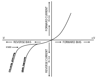
Avalanche breakdown is a phenomenon that can occur in both insulating and semiconducting materials. It is a form of electric current multiplication that can allow very large currents within materials which are otherwise good insulators. It is a type of electron avalanche. The avalanche process occurs when carriers in the transition region are accelerated by the electric field to energies sufficient to create mobile or free electron-hole pairs via collisions with bound electrons.

Explanation
Materials conduct electricity if they contain mobile charge carriers. There are two types of charge carriers in a semiconductor: free electrons (mobile electrons) and electron holes (mobile holes which are missing electrons from the normally occupied electron states). A normally bound electron (e.g., in a bond) in a reverse-biased diode may break loose due to a thermal fluctuation or excitation, creating a mobile electron-hole pair. If there is a voltage gradient (electric field) in the semiconductor, the electron will move towards the positive voltage while the hole will move towards the negative voltage. Usually, the electron and hole will simply move to opposite ends of the crystal and enter the appropriate electrodes. When the electric field is strong enough, the mobile electron or hole may be accelerated to high enough speeds to knock other bound electrons free, creating more free charge carriers, increasing the current and leading to further "knocking out" processes and creating an avalanche. In this way, large portions of a normally insulating crystal can begin to conduct.
The large voltage drop and possibly large current during breakdown necessarily leads to the generation of heat. Therefore, a diode placed into a reverse blocking power application will usually be destroyed by breakdown if the external circuit allows a large current. In principle, avalanche breakdown only involves the passage of electrons and need not cause damage to the crystal. Avalanche diodes (commonly encountered as high voltage Zener diodes) are constructed to break down at a uniform voltage and to avoid current crowding during breakdown. These diodes can indefinitely sustain a moderate level of current during breakdown.
The voltage at which the breakdown occurs is called the breakdown voltage. There is a hysteresis effect; once avalanche breakdown has occurred, the material will continue to conduct even if the voltage across it drops below the breakdown voltage. This is different from a Zener diode, which will stop conducting once the reverse voltage drops below the breakdown voltage.
See also
- QBD (electronics)
- Single-photon avalanche diode
- Spark gap
- Zener breakdown
References
- Microelectronic Circuit Design — Richard C Jaeger — ISBN 0-07-114386-6
- The Art of Electronics — Horowitz & Hill — ISBN 0-521-37095-7
- University of Colorado guide to Advance MOSFET design
- McKay, K. (1954). "Avalanche Breakdown in Silicon". Physical Review. 94 (4): 877. Bibcode:1954PhRv...94..877M. doi:10.1103/PhysRev.94.877.
- Power MOSFET avalanche characteristics and ratings - ST Application Note AN2344
- Power MOSFET Avalanche Design Guidelines - Vishay Application Note AN-1005