Characterization (materials science)
Characterization, when used in materials science, refers to the broad and general process by which a material's structure and properties are probed and measured. It is a fundamental process in the field of materials science, without which no scientific understanding of engineering materials could be ascertained.[1][2] The scope of the term often differs; some definitions limit the term's use to techniques which study the microscopic structure and properties of materials,[2] while others use the term to refer to any materials analysis process including macroscopic techniques such as mechanical testing, thermal analysis and density calculation.[3] The scale of the structures observed in materials characterization ranges from angstroms, such as in the imaging of individual atoms and chemical bonds, up to centimeters, such as in the imaging of coarse grain structures in metals.
While many characterization techniques have been practiced for centuries, such as basic optical microscopy, new techniques and methodologies are constantly emerging. In particular the advent of the electron microscope and Secondary ion mass spectrometry in the 20th century has revolutionized the field, allowing the imaging and analysis of structures and compositions on much smaller scales than was previously possible, leading to a huge increase in the level of understanding as to why different materials show different properties and behaviors.[4] More recently, atomic force microscopy has further increased the maximum possible resolution for analysis of certain samples in the last 30 years.[5]
Microscopy


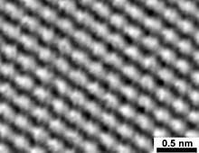
Microscopy is a category of characterization techniques which probe and map the surface and sub-surface structure of a material. These techniques can use photons , electrons , ions or physical cantilever probes to gather data about a sample's structure on a range of length scales. Some common examples of microscopy instruments include:
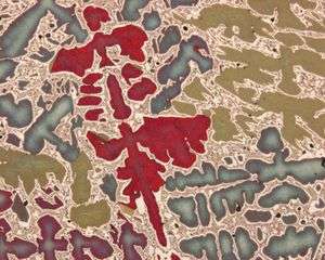
- Optical Microscope
- Scanning Electron Microscope (SEM)
- Transmission Electron Microscope (TEM)
- Field Ion Microscope (FIM)
- Scanning Tunneling Microscope (STM)
- Scanning probe microscopy (SPM)
- Atomic Force Microscope (AFM)
- X-ray diffraction topography (XRT)
Spectroscopy
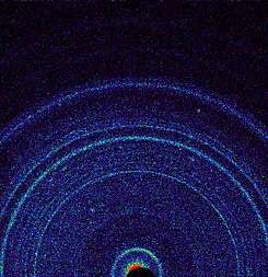
This group of techniques use a range of principles to reveal the chemical composition, composition variation, crystal structure and photoelectric properties of materials. Some common instruments include:
Optical radiation
- Ultraviolet-visible spectroscopy (UV-vis)
- Fourier transform infrared spectroscopy (FTIR)
- Thermoluminescence (TL)
- Photoluminescence (PL)
X-ray

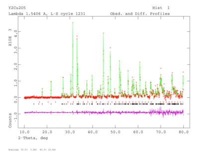
- X-ray diffraction (XRD)
- Small-angle X-ray scattering (SAXS)
- Energy-dispersive X-ray spectroscopy (EDX, EDS)
- Wavelength dispersive X-ray spectroscopy (WDX, WDS)
- Electron energy loss spectroscopy (EELS)
- X-ray photoelectron spectroscopy (XPS)
- Auger electron spectroscopy (AES)
- X-ray Photon Correlation Spectroscopy (XPCS)[6]
Mass spectrometry
- modes of MS:
- Secondary ion mass spectrometry (SIMS)
Nuclear spectroscopy

Other
- Photon correlation spectroscopy/Dynamic light scattering (DLS)
- Terahertz spectroscopy (THz)
- electron paramagnetic/spin resonance (EPR, ESR)
- Small-angle neutron scattering (SANS)
- Rutherford backscattering spectrometry (RBS)
Macroscopic testing
A huge range of techniques are used to characterize various macroscopic properties of materials, including:
- Mechanical testing, including tensile, compressive, torsional, creep, fatigue, toughness and hardness testing
- Differential thermal analysis (DTA)
- Dielectric thermal analysis (DEA, DETA)
- Thermogravimetric analysis (TGA)
- Differential scanning calorimetry (DSC)
- Impulse excitation technique (IET)
- Ultrasound techniques, including resonant ultrasound spectroscopy and time domain ultrasonic testing methods[7]
_effective_refractive_indexes_and_(b)_absorption_coefficients_of_the_electronic_chips.jpg)
See also
References
- Kumar, Sam Zhang, Lin Li, Ashok (2009). Materials characterization techniques. Boca Raton: CRC Press. ISBN 978-1420042948.
- Leng, Yang (2009). Materials Characterization: Introduction to Microscopic and Spectroscopic Methods. Wiley. ISBN 978-0-470-82299-9.
- Zhang, Sam (2008). Materials Characterization Techniques. CRC Press. ISBN 978-1420042948.
- Mathys, Daniel, Zentrum für Mikroskopie, University of Basel: Die Entwicklung der Elektronenmikroskopie vom Bild über die Analyse zum Nanolabor, p. 8
- Patent US4724318 - Atomic force microscope and method for imaging surfaces with atomic resolution - Google Patents
- "What is X-ray Photon Correlation Spectroscopy (XPCS)?". sector7.xray.aps.anl.gov. Archived from the original on 2018-08-22. Retrieved 2016-10-29.
- R. Truell, C. Elbaum and C.B. Chick., Ultrasonic methods in solid state physics New York, Academic Press Inc., 1969.
- Ahi, Kiarash; Shahbazmohamadi, Sina; Asadizanjani, Navid (2018). "Quality control and authentication of packaged integrated circuits using enhanced-spatial-resolution terahertz time-domain spectroscopy and imaging". Optics and Lasers in Engineering. 104: 274–284. Bibcode:2018OptLE.104..274A. doi:10.1016/j.optlaseng.2017.07.007.
