History of nanotechnology
The history of nanotechnology traces the development of the concepts and experimental work falling under the broad category of nanotechnology. Although nanotechnology is a relatively recent development in scientific research, the development of its central concepts happened over a longer period of time. The emergence of nanotechnology in the 1980s was caused by the convergence of experimental advances such as the invention of the scanning tunneling microscope in 1981 and the discovery of fullerenes in 1985, with the elucidation and popularization of a conceptual framework for the goals of nanotechnology beginning with the 1986 publication of the book Engines of Creation. The field was subject to growing public awareness and controversy in the early 2000s, with prominent debates about both its potential implications as well as the feasibility of the applications envisioned by advocates of molecular nanotechnology, and with governments moving to promote and fund research into nanotechnology. The early 2000s also saw the beginnings of commercial applications of nanotechnology, although these were limited to bulk applications of nanomaterials rather than the transformative applications envisioned by the field.
| Part of a series of articles on |
| Nanotechnology |
|---|
| Impact and applications |
| Nanomaterials |
| Molecular self-assembly |
| Nanoelectronics |
| Nanometrology |
|
| Molecular nanotechnology |
|
Early uses of nanomaterials
The earliest evidence of the use and applications of nanotechnology can be traced back to carbon nanotubes, cementite nanowires found in the microstructure of wootz steel manufactured in ancient India from the time period of 600 BC and exported globally.[1]
Although nanoparticles are associated with modern science, they were used by artisans as far back as the ninth century in Mesopotamia for creating a glittering effect on the surface of pots.[2][3]
In modern times, pottery from the Middle Ages and Renaissance often retains a distinct gold- or copper-colored metallic glitter. This luster is caused by a metallic film that was applied to the transparent surface of a glazing, which contains silver and copper nanoparticles dispersed homogeneously in the glassy matrix of the ceramic glaze. These nanoparticles are created by the artisans by adding copper and silver salts and oxides together with vinegar, ochre, and clay on the surface of previously-glazed pottery. The technique originated in the Muslim world. As Muslims were not allowed to use gold in artistic representations, they sought a way to create a similar effect without using real gold. The solution they found was using luster.[3][4]
Conceptual origins
Richard Feynman

The American physicist Richard Feynman lectured, "There's Plenty of Room at the Bottom," at an American Physical Society meeting at Caltech on December 29, 1959, which is often held to have provided inspiration for the field of nanotechnology. Feynman had described a process by which the ability to manipulate individual atoms and molecules might be developed, using one set of precise tools to build and operate another proportionally smaller set, so on down to the needed scale. In the course of this, he noted, scaling issues would arise from the changing magnitude of various physical phenomena: gravity would become less important, surface tension and Van der Waals attraction would become more important.[5]
After Feynman's death, a scholar studying the historical development of nanotechnology has concluded that his actual role in catalyzing nanotechnology research was limited, based on recollections from many of the people active in the nascent field in the 1980s and 1990s. Chris Toumey, a cultural anthropologist at the University of South Carolina, found that the published versions of Feynman’s talk had a negligible influence in the twenty years after it was first published, as measured by citations in the scientific literature, and not much more influence in the decade after the Scanning Tunneling Microscope was invented in 1981. Subsequently, interest in “Plenty of Room” in the scientific literature greatly increased in the early 1990s. This is probably because the term “nanotechnology” gained serious attention just before that time, following its use by K. Eric Drexler in his 1986 book, Engines of Creation: The Coming Era of Nanotechnology, which took the Feynman concept of a billion tiny factories and added the idea that they could make more copies of themselves via computer control instead of control by a human operator; and in a cover article headlined "Nanotechnology",[6][7] published later that year in a mass-circulation science-oriented magazine, Omni. Toumey’s analysis also includes comments from distinguished scientists in nanotechnology who say that “Plenty of Room” did not influence their early work, and in fact most of them had not read it until a later date.[8][9]
These and other developments hint that the retroactive rediscovery of Feynman’s “Plenty of Room” gave nanotechnology a packaged history that provided an early date of December 1959, plus a connection to the charisma and genius of Richard Feynman. Feynman's stature as a Nobel laureate and as an iconic figure in 20th century science surely helped advocates of nanotechnology and provided a valuable intellectual link to the past.[10]
Norio Taniguchi
The Japanese scientist called Norio Taniguchi of Tokyo University of Science was first to use the term "nano-technology" in a 1974 conference,[11] to describe semiconductor processes such as thin film deposition and ion beam milling exhibiting characteristic control on the order of a nanometer. His definition was, "'Nano-technology' mainly consists of the processing of, separation, consolidation, and deformation of materials by one atom or one molecule." However, the term was not used again until 1981 when Eric Drexler, who was unaware of Taniguchi's prior use of the term, published his first paper on nanotechnology in 1981.[12][13][14]
K. Eric Drexler

In the 1980s the idea of nanotechnology as a deterministic, rather than stochastic, handling of individual atoms and molecules was conceptually explored in depth by K. Eric Drexler, who promoted the technological significance of nano-scale phenomena and devices through speeches and two influential books.
In 1980, Drexler encountered Feynman's provocative 1959 talk "There's Plenty of Room at the Bottom" while preparing his initial scientific paper on the subject, “Molecular Engineering: An approach to the development of general capabilities for molecular manipulation,” published in the Proceedings of the National Academy of Sciences in 1981.[15] The term "nanotechnology" (which paralleled Taniguchi's "nano-technology") was independently applied by Drexler in his 1986 book Engines of Creation: The Coming Era of Nanotechnology, which proposed the idea of a nanoscale "assembler" which would be able to build a copy of itself and of other items of arbitrary complexity. He also first published the term "grey goo" to describe what might happen if a hypothetical self-replicating machine, capable of independent operation, were constructed and released. Drexler's vision of nanotechnology is often called "Molecular Nanotechnology" (MNT) or "molecular manufacturing."
His 1991 Ph.D. work at the MIT Media Lab was the first doctoral degree on the topic of molecular nanotechnology and (after some editing) his thesis, "Molecular Machinery and Manufacturing with Applications to Computation,"[16] was published as Nanosystems: Molecular Machinery, Manufacturing, and Computation,[17] which received the Association of American Publishers award for Best Computer Science Book of 1992. Drexler founded the Foresight Institute in 1986 with the mission of "Preparing for nanotechnology.” Drexler is no longer a member of the Foresight Institute.
Experimental research and advances
In nanoelectronics, nanoscale thickness was demonstrated in the gate oxide and thin films used in transistors as early as the 1960s, but it was not until the late 1990s that MOSFETs (metal–oxide–semiconductor field-effect transistors) with nanoscale gate length were demonstrated. Nanotechnology and nanoscience got a boost in the early 1980s with two major developments: the birth of cluster science and the invention of the scanning tunneling microscope (STM). These developments led to the discovery of fullerenes in 1985 and the structural assignment of carbon nanotubes in 1991. The development of FinFET in the 1990s aldo laid the foundations for modern nanoelectronic semiconductor device fabrication.
Nanoscale transistors
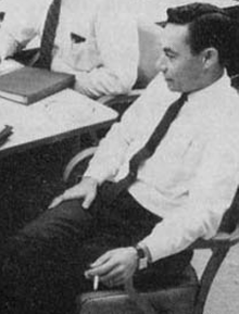
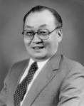
In 1960, Egyptian engineer Mohamed Atalla and Korean engineer Dawon Kahng at Bell Labs fabricated the first MOSFET (metal–oxide–semiconductor field-effect transistor) with a gate oxide thickness of 100 nm, along with a gate length of 20 µm.[18] In 1962, Atalla and Kahng fabricated a nanolayer-base metal–semiconductor junction (M–S junction) transistor that used gold (Au) thin films with a thickness of 10 nm.[19] In 1987, Iranian engineer Bijan Davari led an IBM research team that demonstrated the first MOSFET with a 10 nm gate oxide thickness, using tungsten-gate technology.[20]
Multi-gate MOSFETs enabled scaling below 20 nm gate length, starting with the FinFET (fin field-effect transistor), a three-dimensional, non-planar, double-gate MOSFET.[21] The FinFET originates from the DELTA transistor developed by Hitachi Central Research Laboratory's Digh Hisamoto, Toru Kaga, Yoshifumi Kawamoto and Eiji Takeda in 1989.[22][23][24][25] In 1997, DARPA awarded a contract to a research group at UC Berkeley to develop a deep sub-micron DELTA transistor.[25] The group consisted of Hisamoto along with TSMC's Chenming Hu and other international researchers including Tsu-Jae King Liu, Jeffrey Bokor, Hideki Takeuchi, K. Asano, Jakub Kedziersk, Xuejue Huang, Leland Chang, Nick Lindert, Shibly Ahmed and Cyrus Tabery. The team successfully fabricated FinFET devices down to a 17 nm process in 1998, and then 15 nm in 2001. In 2002, a team including Yu, Chang, Ahmed, Hu, Liu, Bokor and Tabery fabricated a 10 nm FinFET device.[21]
In 2006, a team of Korean researchers from the Korea Advanced Institute of Science and Technology (KAIST) and the National Nano Fab Center developed a 3 nm MOSFET, the world's smallest nanoelectronic device. It was based on gate-all-around (GAA) FinFET technology.[26][27]
Invention of scanning probe microscopy

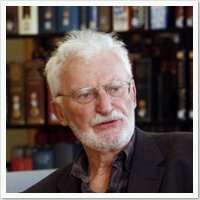
The scanning tunneling microscope, an instrument for imaging surfaces at the atomic level, was developed in 1981 by Gerd Binnig and Heinrich Rohrer at IBM Zurich Research Laboratory, for which they were awarded the Nobel Prize in Physics in 1986.[28][29] Binnig, Calvin Quate and Christoph Gerber invented the first atomic force microscope in 1986. The first commercially available atomic force microscope was introduced in 1989.
IBM researcher Don Eigler was the first to manipulate atoms using a scanning tunneling microscope in 1989. He used 35 Xenon atoms to spell out the IBM logo.[30] He shared the 2010 Kavli Prize in Nanoscience for this work.[31]
Advances in interface and colloid science
Interface and colloid science had existed for nearly a century before they became associated with nanotechnology.[32][33] The first observations and size measurements of nanoparticles had been made during the first decade of the 20th century by Richard Adolf Zsigmondy, winner of the 1925 Nobel Prize in Chemistry, who made a detailed study of gold sols and other nanomaterials with sizes down to 10 nm using an ultramicroscope which was capable of visualizing particles much smaller than the light wavelength.[34] Zsigmondy was also the first to use the term "nanometer" explicitly for characterizing particle size. In the 1920s, Irving Langmuir, winner of the 1932 Nobel Prize in Chemistry, and Katharine B. Blodgett introduced the concept of a monolayer, a layer of material one molecule thick. In the early 1950s, Derjaguin and Abrikosova conducted the first measurement of surface forces.[35]
In 1974 the process of atomic layer deposition for depositing uniform thin films one atomic layer at a time was developed and patented by Tuomo Suntola and co-workers in Finland.[36]
In another development, the synthesis and properties of semiconductor nanocrystals were studied. This led to a fast increasing number of semiconductor nanoparticles of quantum dots.
Discovery of fullerenes

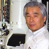
Fullerenes were discovered in 1985 by Harry Kroto, Richard Smalley, and Robert Curl, who together won the 1996 Nobel Prize in Chemistry. Smalley's research in physical chemistry investigated formation of inorganic and semiconductor clusters using pulsed molecular beams and time of flight mass spectrometry. As a consequence of this expertise, Curl introduced him to Kroto in order to investigate a question about the constituents of astronomical dust. These are carbon rich grains expelled by old stars such as R Corona Borealis. The result of this collaboration was the discovery of C60 and the fullerenes as the third allotropic form of carbon. Subsequent discoveries included the endohedral fullerenes, and the larger family of fullerenes the following year.[37][38]
The discovery of carbon nanotubes is largely attributed to Sumio Iijima of NEC in 1991, although carbon nanotubes have been produced and observed under a variety of conditions prior to 1991.[39] Iijima's discovery of multi-walled carbon nanotubes in the insoluble material of arc-burned graphite rods in 1991[40] and Mintmire, Dunlap, and White's independent prediction that if single-walled carbon nanotubes could be made, then they would exhibit remarkable conducting properties[41] helped create the initial buzz that is now associated with carbon nanotubes. Nanotube research accelerated greatly following the independent discoveries[42][43] by Bethune at IBM[44] and Iijima at NEC of single-walled carbon nanotubes and methods to specifically produce them by adding transition-metal catalysts to the carbon in an arc discharge.
In the early 1990s Huffman and Kraetschmer, of the University of Arizona, discovered how to synthesize and purify large quantities of fullerenes. This opened the door to their characterization and functionalization by hundreds of investigators in government and industrial laboratories. Shortly after, rubidium doped C60 was found to be a mid temperature (Tc = 32 K) superconductor. At a meeting of the Materials Research Society in 1992, Dr. T. Ebbesen (NEC) described to a spellbound audience his discovery and characterization of carbon nanotubes. This event sent those in attendance and others downwind of his presentation into their laboratories to reproduce and push those discoveries forward. Using the same or similar tools as those used by Huffman and Kratschmer, hundreds of researchers further developed the field of nanotube-based nanotechnology.
Government and corporate support
National Nanotechnology Initiative

The National Nanotechnology Initiative is a United States federal nanotechnology research and development program. “The NNI serves as the central point of communication, cooperation, and collaboration for all Federal agencies engaged in nanotechnology research, bringing together the expertise needed to advance this broad and complex field."[45] Its goals are to advance a world-class nanotechnology research and development (R&D) program, foster the transfer of new technologies into products for commercial and public benefit, develop and sustain educational resources, a skilled workforce, and the supporting infrastructure and tools to advance nanotechnology, and support responsible development of nanotechnology. The initiative was spearheaded by Mihail Roco, who formally proposed the National Nanotechnology Initiative to the Office of Science and Technology Policy during the Clinton administration in 1999, and was a key architect in its development. He is currently the Senior Advisor for Nanotechnology at the National Science Foundation, as well as the founding chair of the National Science and Technology Council subcommittee on Nanoscale Science, Engineering and Technology.[46]
President Bill Clinton advocated nanotechnology development. In a 21 January 2000 speech[47] at the California Institute of Technology, Clinton said, "Some of our research goals may take twenty or more years to achieve, but that is precisely why there is an important role for the federal government." Feynman's stature and concept of atomically precise fabrication played a role in securing funding for nanotechnology research, as mentioned in President Clinton's speech:
My budget supports a major new National Nanotechnology Initiative, worth $500 million. Caltech is no stranger to the idea of nanotechnology the ability to manipulate matter at the atomic and molecular level. Over 40 years ago, Caltech's own Richard Feynman asked, "What would happen if we could arrange the atoms one by one the way we want them?"[48]
President George W. Bush further increased funding for nanotechnology. On December 3, 2003 Bush signed into law the 21st Century Nanotechnology Research and Development Act,[49] which authorizes expenditures for five of the participating agencies totaling US$3.63 billion over four years.[50] The NNI budget supplement for Fiscal Year 2009 provides $1.5 billion to the NNI, reflecting steady growth in the nanotechnology investment.[51]
Other international government and corporate support
Over sixty countries created nanotechnology research and development (R&D) government programs between 2001 and 2004. Government funding was exceeded by corporate spending on nanotechnology R&D, with most of the funding coming from corporations based in the United States, Japan and Germany. The top five organizations that filed the most intellectual patents on nanotechnology R&D between 1970 and 2011 were Samsung Electronics (2,578 first patents), Nippon Steel (1,490 first patents), IBM (1,360 first patents), Toshiba (1,298 first patents) and Canon (1,162 first patents). The top five organizations that published the most scientific papers on nanotechnology research between 1970 and 2012 were the Chinese Academy of Sciences, Russian Academy of Sciences, Centre national de la recherche scientifique, University of Tokyo and Osaka University.[52]
Growing public awareness and controversy
"Why the future doesn't need us"
"Why the future doesn't need us" is an article written by Bill Joy, then Chief Scientist at Sun Microsystems, in the April 2000 issue of Wired magazine. In the article, he argues that "Our most powerful 21st-century technologies — robotics, genetic engineering, and nanotech — are threatening to make humans an endangered species." Joy argues that developing technologies provide a much greater danger to humanity than any technology before it has ever presented. In particular, he focuses on genetics, nanotechnology and robotics. He argues that 20th-century technologies of destruction, such as the nuclear bomb, were limited to large governments, due to the complexity and cost of such devices, as well as the difficulty in acquiring the required materials. He also voices concern about increasing computer power. His worry is that computers will eventually become more intelligent than we are, leading to such dystopian scenarios as robot rebellion. He notably quotes the Unabomber on this topic. After the publication of the article, Bill Joy suggested assessing technologies to gauge their implicit dangers, as well as having scientists refuse to work on technologies that have the potential to cause harm.
In the AAAS Science and Technology Policy Yearbook 2001 article titled A Response to Bill Joy and the Doom-and-Gloom Technofuturists, Bill Joy was criticized for having technological tunnel vision on his prediction, by failing to consider social factors.[53] In Ray Kurzweil's The Singularity Is Near, he questioned the regulation of potentially dangerous technology, asking "Should we tell the millions of people afflicted with cancer and other devastating conditions that we are canceling the development of all bioengineered treatments because there is a risk that these same technologies may someday be used for malevolent purposes?".
Prey
Prey is a 2002 novel by Michael Crichton which features an artificial swarm of nanorobots which develop intelligence and threaten their human inventors. The novel generated concern within the nanotechnology community that the novel could negatively affect public perception of nanotechnology by creating fear of a similar scenario in real life.[54]
Drexler–Smalley debate
Richard Smalley, best known for co-discovering the soccer ball-shaped “buckyball” molecule and a leading advocate of nanotechnology and its many applications, was an outspoken critic of the idea of molecular assemblers, as advocated by Eric Drexler. In 2001 he introduced scientific objections to them[55] attacking the notion of universal assemblers in a 2001 Scientific American article, leading to a rebuttal later that year from Drexler and colleagues,[56] and eventually to an exchange of open letters in 2003.[57]
Smalley criticized Drexler's work on nanotechnology as naive, arguing that chemistry is extremely complicated, reactions are hard to control, and that a universal assembler is science fiction. Smalley believed that such assemblers were not physically possible and introduced scientific objections to them. His two principal technical objections, which he had termed the “fat fingers problem" and the "sticky fingers problem”, argued against the feasibility of molecular assemblers being able to precisely select and place individual atoms. He also believed that Drexler’s speculations about apocalyptic dangers of molecular assemblers threaten the public support for development of nanotechnology.
Smalley first argued that "fat fingers" made MNT impossible. He later argued that nanomachines would have to resemble chemical enzymes more than Drexler's assemblers and could only work in water. He believed these would exclude the possibility of "molecular assemblers" that worked by precision picking and placing of individual atoms. Also, Smalley argued that nearly all of modern chemistry involves reactions that take place in a solvent (usually water), because the small molecules of a solvent contribute many things, such as lowering binding energies for transition states. Since nearly all known chemistry requires a solvent, Smalley felt that Drexler's proposal to use a high vacuum environment was not feasible.
Smalley also believed that Drexler's speculations about apocalyptic dangers of self-replicating machines that have been equated with "molecular assemblers" would threaten the public support for development of nanotechnology. To address the debate between Drexler and Smalley regarding molecular assemblers Chemical & Engineering News published a point-counterpoint consisting of an exchange of letters that addressed the issues.[57]
Drexler and coworkers responded to these two issues[56] in a 2001 publication. Drexler and colleagues noted that Drexler never proposed universal assemblers able to make absolutely anything, but instead proposed more limited assemblers able to make a very wide variety of things. They challenged the relevance of Smalley's arguments to the more specific proposals advanced in Nanosystems. Drexler maintained that both were straw man arguments, and in the case of enzymes, Prof. Klibanov wrote in 1994, "...using an enzyme in organic solvents eliminates several obstacles..."[58] Drexler also addresses this in Nanosystems by showing mathematically that well designed catalysts can provide the effects of a solvent and can fundamentally be made even more efficient than a solvent/enzyme reaction could ever be. Drexler had difficulty in getting Smalley to respond, but in December 2003, Chemical & Engineering News carried a 4-part debate.[57]
Ray Kurzweil spends four pages in his book 'The Singularity Is Near' to showing that Richard Smalley's arguments are not valid, and disputing them point by point. Kurzweil ends by stating that Drexler's visions are very practicable and even happening already.[59]
Royal Society report on the implications of nanotechnology
The Royal Society and Royal Academy of Engineering's 2004 report on the implications of nanoscience and nanotechnologies[60] was inspired by Prince Charles' concerns about nanotechnology, including molecular manufacturing. However, the report spent almost no time on molecular manufacturing.[61] In fact, the word "Drexler" appears only once in the body of the report (in passing), and "molecular manufacturing" or "molecular nanotechnology" not at all. The report covers various risks of nanoscale technologies, such as nanoparticle toxicology. It also provides a useful overview of several nanoscale fields. The report contains an annex (appendix) on grey goo, which cites a weaker variation of Richard Smalley's contested argument against molecular manufacturing. It concludes that there is no evidence that autonomous, self replicating nanomachines will be developed in the foreseeable future, and suggests that regulators should be more concerned with issues of nanoparticle toxicology.
Initial commercial applications
The early 2000s saw the beginnings of the use of nanotechnology in commercial products, although most applications are limited to the bulk use of passive nanomaterials. Examples include titanium dioxide and zinc oxide nanoparticles in sunscreen, cosmetics and some food products; silver nanoparticles in food packaging, clothing, disinfectants and household appliances such as Silver Nano; carbon nanotubes for stain-resistant textiles; and cerium oxide as a fuel catalyst.[62] As of March 10, 2011, the Project on Emerging Nanotechnologies estimated that over 1300 manufacturer-identified nanotech products are publicly available, with new ones hitting the market at a pace of 3–4 per week.[63]
The National Science Foundation funded researcher David Berube to study the field of nanotechnology. His findings are published in the monograph Nano-Hype: The Truth Behind the Nanotechnology Buzz. This study concludes that much of what is sold as “nanotechnology” is in fact a recasting of straightforward materials science, which is leading to a “nanotech industry built solely on selling nanotubes, nanowires, and the like” which will “end up with a few suppliers selling low margin products in huge volumes." Further applications which require actual manipulation or arrangement of nanoscale components await further research. Though technologies branded with the term 'nano' are sometimes little related to and fall far short of the most ambitious and transformative technological goals of the sort in molecular manufacturing proposals, the term still connotes such ideas. According to Berube, there may be a danger that a "nano bubble" will form, or is forming already, from the use of the term by scientists and entrepreneurs to garner funding, regardless of interest in the transformative possibilities of more ambitious and far-sighted work.[64]
Commercial nanoelectronic semiconductor device fabrication began in the 2010s. In 2013, SK Hynix began commercial mass-production of a 16 nm process,[65] TSMC began production of a 16 nm FinFET process,[66] and Samsung Electronics began production of a 10 nm process.[67] TSMC began production of a 7 nm process in 2017,[68] and Samsung began production of a 5 nm process in 2018.[69] In 2019, Samsung announced plans for the commercial production of a 3 nm GAAFET process by 2021.[70]
References
- Sanderson, Katharine (2006-11-15). "Sharpest cut from nanotube sword". Nature News. doi:10.1038/news061113-11.
- Reiss, Gunter; Hutten, Andreas (2010). "Magnetic Nanoparticles". In Sattler, Klaus D. (ed.). Handbook of Nanophysics: Nanoparticles and Quantum Dots. CRC Press. pp. 2–1. ISBN 9781420075458.
- Khan, Firdos Alam (2012). Biotechnology Fundamentals. CRC Press. p. 328. ISBN 9781439820094.
- Rawson, Philip S. (1984). Ceramics. University of Pennsylvania Press. ISBN 978-0-8122-1156-6.
- Gribbin, John; Gribbin, Mary (1997). Richard Feynman: A Life in Science. Dutton. p. 170. ISBN 978-0-452-27631-4.
- Hapgood, Fred (November 1986). ""Nanotechnology" / "Tinytech"". Omni: 56.
- Drexler, Eric (15 December 2009). "The promise that launched the field of nanotechnology". Metamodern: The Trajectory of Technology. Archived from the original on 14 July 2011. Retrieved 13 May 2011.
- Toumey, Chris (2005). "Apostolic Succession" (PDF). Engineering & Science. 1/2: 16–23.
- Toumey, Chris (2008). "Reading Feynman into Nanotechnology: A Text for a New Science" (PDF). Techné. 13 (3): 133–168. Archived from the original (PDF) on 2009-09-19.
- Milburn, Colin (2008). Nanovision: Engineering the Future. Duke University Press. ISBN 978-0-8223-4265-6.
- Taniguchi, Norio (1974). "On the Basic Concept of 'Nano-Technology'". Proceedings of the International Conference on Production Engineering, Tokyo, 1974, Part II.
- Bassett, Deborah R. (2010). "Taniguchi, Norio". In Guston, David H. (ed.). Encyclopedia of nanoscience and society. London: SAGE. p. 747. ISBN 9781452266176. Retrieved 3 August 2014.
- Koodali, Ranjit T.; Klabunde, Kenneth J. (2012). "Nanotechnology: Fandamental Principles and Applications". In Kent, James A. (ed.). Handbook of industrial chemistry and biotechnology, volume 1 (12th ed.). New York: Springer. p. 250. ISBN 9781461442592. Retrieved 3 August 2014.
- Maynard, edited by Graeme A. Hodge, Diana M. Bowman, Andrew D. (2010). "Tracing and disputing the story of nanotechnology". In Hodge, Graeme A.; Bowman, Diana M.; Maynard, Andrew D. (eds.). International handbook on regulating nanotechnologies. Cheltenham, UK: Edward Elgar. p. 54. ISBN 9781849808125. Retrieved 4 August 2014.CS1 maint: extra text: authors list (link)
- Drexler, K. E. (1981). "Molecular engineering: An approach to the development of general capabilities for molecular manipulation". Proceedings of the National Academy of Sciences of the United States of America. 78 (9): 5275–5278. Bibcode:1981PNAS...78.5275D. doi:10.1073/pnas.78.9.5275. PMC 348724. PMID 16593078.
- Drexler, K. Eric. Molecular Machinery and Manufacturing with Applications to Computation (PDF) (Ph.D. thesis). Massachusetts Institute of Technology. Archived from the original (PDF) on 2008-09-08.
- Drexler, K. Eric (1992). Nanosystems: Molecular Machinery, Manufacturing, and Computation. Wiley. ISBN 978-0-471-57518-4. Retrieved 14 May 2011.
- Sze, Simon M. (2002). Semiconductor Devices: Physics and Technology (PDF) (2nd ed.). Wiley. p. 4. ISBN 0-471-33372-7.
- Pasa, André Avelino (2010). "Chapter 13: Metal Nanolayer-Base Transistor". Handbook of Nanophysics: Nanoelectronics and Nanophotonics. CRC Press. pp. 13–1, 13–4. ISBN 9781420075519.
- Davari, Bijan; Ting, Chung-Yu; Ahn, Kie Y.; Basavaiah, S.; Hu, Chao-Kun; Taur, Yuan; Wordeman, Matthew R.; Aboelfotoh, O.; Krusin-Elbaum, L.; Joshi, Rajiv V.; Polcari, Michael R. (1987). "Submicron Tungsten Gate MOSFET with 10 nm Gate Oxide". 1987 Symposium on VLSI Technology. Digest of Technical Papers: 61–62.
- Tsu‐Jae King, Liu (June 11, 2012). "FinFET: History, Fundamentals and Future". University of California, Berkeley. Symposium on VLSI Technology Short Course. Retrieved 9 July 2019.
- Colinge, J.P. (2008). FinFETs and Other Multi-Gate Transistors. Springer Science & Business Media. p. 11. ISBN 9780387717517.
- Hisamoto, D.; Kaga, T.; Kawamoto, Y.; Takeda, E. (December 1989). "A fully depleted lean-channel transistor (DELTA)-a novel vertical ultra thin SOI MOSFET". International Technical Digest on Electron Devices Meeting: 833–836. doi:10.1109/IEDM.1989.74182.
- "IEEE Andrew S. Grove Award Recipients". IEEE Andrew S. Grove Award. Institute of Electrical and Electronics Engineers. Retrieved 4 July 2019.
- "The Breakthrough Advantage for FPGAs with Tri-Gate Technology" (PDF). Intel. 2014. Retrieved 4 July 2019.
- "Still Room at the Bottom (nanometer transistor developed by Yang-kyu Choi from the Korea Advanced Institute of Science and Technology)", Nanoparticle News, 1 April 2006, archived from the original on 6 November 2012
- Lee, Hyunjin; et al. (2006), "Sub-5nm All-Around Gate FinFET for Ultimate Scaling", Symposium on VLSI Technology, 2006: 58–59, doi:10.1109/VLSIT.2006.1705215, hdl:10203/698, ISBN 978-1-4244-0005-8
- Binnig, G.; Rohrer, H. (1986). "Scanning tunneling microscopy". IBM Journal of Research and Development. 30 (4): 355–69.
- "Press Release: the 1996 Nobel Prize in Physics". Nobelprize.org. 15 October 1986. Retrieved 12 May 2011.
- Shankland, Stephen (28 September 2009). "IBM's 35 atoms and the rise of nanotech". CNET. Retrieved 12 May 2011.
- "The Kavli Prize Laureates 2010". The Norwegian Academy of Science and Letters. Archived from the original on 12 May 2011. Retrieved 13 May 2011.
- Efremov, I.F. (1976). "Periodic Colloidal Structures". In Matijevic, E. (ed.). Surface and Colloid Science. 8. New York: Wiley.
- Lyklema, J. (2000). Fundamentals of Interface and Colloid Science. Academic Press. ISBN 978-0-12-460523-7. Archived from the original on 2012-10-12. Retrieved 2011-05-12.
- Zsigmondy, R. (1914). Colloids and the Ultramicroscope. New York: J.Wiley and Sons. Retrieved 10 May 2011.
- Derjaguin, B. V.; Titijevskaia, A. S.; Abricossova, I. I.; Malkina, A. D. (1954). "Investigations of the forces of interaction of surfaces in different media and their application to the problem of colloid stability". Discussions of the Faraday Society. 18: 24. doi:10.1039/DF9541800024.
- "History of Atomic Layer Deposition". Finnish Micro & Nano Technology Network. Archived from the original on 28 September 2007.
- Kroto, H. W.; Heath, J. R.; O'Brien, S. C.; Curl, R. F.; Smalley, R. E. (1985). "C60: Buckminsterfullerene". Nature. 318 (6042): 162–163. Bibcode:1985Natur.318..162K. doi:10.1038/318162a0.
- Adams, W Wade; Baughman, Ray H (2005). "Retrospective: Richard E. Smalley (1943–2005)". Science. 310 (5756) (published Dec 23, 2005). p. 1916. doi:10.1126/science.1122120. PMID 16373566.
- Monthioux, Marc; Kuznetsov, V (2006). "Who should be given the credit for the discovery of carbon nanotubes?" (PDF). Carbon. 44 (9): 1621–1623. doi:10.1016/j.carbon.2006.03.019.
- Iijima, Sumio (7 November 1991). "Helical microtubules of graphitic carbon". Nature. 354 (6348): 56–58. Bibcode:1991Natur.354...56I. doi:10.1038/354056a0.
- Mintmire, J.W.; Dunlap, BI; White, CT (1992). "Are Fullerene Tubules Metallic?". Physical Review Letters. 68 (5): 631–634. Bibcode:1992PhRvL..68..631M. doi:10.1103/PhysRevLett.68.631. PMID 10045950.
- Bethune, D. S.; Klang, C. H.; De Vries, M. S.; Gorman, G.; Savoy, R.; Vazquez, J.; Beyers, R. (1993). "Cobalt-catalyzed growth of carbon nanotubes with single-atomic-layer walls". Nature. 363 (6430): 605–607. Bibcode:1993Natur.363..605B. doi:10.1038/363605a0.
- Iijima, Sumio; Ichihashi, Toshinari (1993). "Single-shell carbon nanotubes of 1-nm diameter". Nature. 363 (6430): 603–605. Bibcode:1993Natur.363..603I. doi:10.1038/363603a0.
- "The Discovery of Single-Wall Carbon Nanotubes at IBM". IBM. 2016-07-25.
- "About the NNI | Nano".
- "Dr. Mihail C. Roco, Senior Advisor for Nanotechnology, National Science Foundation". National Science Foundation. Archived from the original on 11 April 2010. Retrieved 8 November 2009.
- "President Clinton's Address to Caltech on Science and Technology". California Institute of Technology. Archived from the original on 7 August 2011. Retrieved 13 May 2011.
- Jones, Richard M. (21 January 2000). "President Requests Significant Increase in FY 2001 Research Budget". FYI: The AIP Bulletin of Science Policy News. American Institute of Physics. Retrieved 13 May 2011.
- "21st Century Nanotechnology Research and Development Act (Public Law 108-153)". United States Government Printing Office. Retrieved 12 May 2011.
- "Remarks Prepared for Delivery: National Nanotechnology Initiative Conference, Senator George Allen, Thursday, April 1, 2004". United States National Nanotechnology Initiative. Archived from the original on 27 September 2007.
- "National Nanotechnology Initiative: FY 2009 Budget & Highlights" (PDF). United States National Nanotechnology Initiative. Archived from the original (PDF) on 27 May 2010.
- World Intellectual Property Report: Breakthrough Innovation and Economic Growth (PDF). World Intellectual Property Organization. 2015. pp. 112–4. Retrieved 9 July 2019.
- Brown, John Seely and Duguid, Paul (13 April 2000). "A Response to Bill Joy and the Doom-and-Gloom Technofuturists" (PDF). Archived from the original (PDF) on 31 December 2003. Retrieved 12 May 2011.CS1 maint: multiple names: authors list (link)
- Edwards, Steven A. (2006). The Nanotech Pioneers: Where Are They Taking Us?. Weinheim: Wiley-VCH. pp. 22–23.
- Smalley, Richard E. (September 2001). "Of Chemistry, Love and Nanobots". Scientific American. 285 (3): 76–7. Bibcode:2001SciAm.285c..76S. doi:10.1038/scientificamerican0901-76. PMID 11524973. Archived from the original on 2012-07-23. Retrieved 2011-05-12.
- Drexler, K. Eric; Forrest, David; Freitas, Robert A.; Hall, J. Storrs; Jacobstein, Neil; McKendree, Tom; Merkle, Ralph; Peterson, Christine (2001). "Debate About Assemblers — Smalley Rebuttal". Institute for Molecular Manufacturing. Retrieved 9 May 2010.
- "Nanotechnology: Drexler and Smalley make the case for and against 'molecular assemblers'". Chemical & Engineering News. 81 (48): 37–42. 1 December 2003. doi:10.1021/cen-v081n036.p037. Retrieved 9 May 2010.
- Phoenix, Chris (December 2003). "Of Chemistry, Nanobots, and Policy". Center for Responsible Nanotechnology. Retrieved 12 May 2011.
- Kurzweil, Ray (2005). The Singularity Is Near. pp. 193–196. ISBN 978-0-670-03384-3.
- "Nanoscience and nanotechnologies: opportunities and uncertainties". Royal Society and Royal Academy of Engineering. July 2004. Archived from the original on 3 July 2018. Retrieved 13 May 2011.
- "Royal Society in Denial". Center for Responsible Nanotechnology. 31 July 2004. Retrieved 13 May 2011.
- "Nanotechnology Information Center: Properties, Applications, Research, and Safety Guidelines". American Elements. Retrieved 13 May 2011.
- "Analysis: This is the first publicly available on-line inventory of nanotechnology-based consumer products". The Project on Emerging Nanotechnologies. 2008. Retrieved 13 May 2011.
- Berube, David (2006). Nano-Hype: The Truth Behind the Nanotechnology Buzz. Amherst, NY: Prometheus Books. Archived from the original on 2017-10-28. Retrieved 2020-01-15.
- "History: 2010s". SK Hynix. Retrieved 8 July 2019.
- "16/12nm Technology". TSMC. Retrieved 30 June 2019.
- "Samsung Mass Producing 128Gb 3-bit MLC NAND Flash". Tom's Hardware. 11 April 2013. Retrieved 21 June 2019.
- "7nm Technology". TSMC. Retrieved 30 June 2019.
- Shilov, Anton. "Samsung Completes Development of 5nm EUV Process Technology". www.anandtech.com. Retrieved 2019-05-31.
- Armasu, Lucian (11 January 2019), "Samsung Plans Mass Production of 3nm GAAFET Chips in 2021", www.tomshardware.com
External links
- T. Mappes; et al. (2012). "The Invention of Immersion Ultramicroscopy in 1912—The Birth of Nanotechnology?". Angewandte Chemie International Edition. 51 (45): 11208–11212. doi:10.1002/anie.201204688. PMID 23065955.
- Who Invented Nanotechnology
- What is Nanotechnology with Full Information
- How to make a career in technology