Nanowire
A nanowire is a nanostructure, with the diameter of the order of a nanometre (10−9 meters). It can also be defined as the ratio of the length to width being greater than 1000. Alternatively, nanowires can be defined as structures that have a thickness or diameter constrained to tens of nanometers or less and an unconstrained length. At these scales, quantum mechanical effects are important—which coined the term "quantum wires". Many different types of nanowires exist, including superconducting (e.g. YBCO[1]), metallic (e.g. Ni, Pt, Au), semiconducting (e.g. silicon nanowires (SiNWs), InP, GaN) and insulating (e.g. SiO2, TiO2). Molecular nanowires are composed of repeating molecular units either organic (e.g. DNA) or inorganic (e.g. Mo6S9−xIx).
| Part of a series of articles on |
| Nanoelectronics |
|---|
| Single-molecule electronics |
| Solid-state nanoelectronics |
| Related approaches |
|
Overview
Typical nanowires exhibit aspect ratios (length-to-width ratio) of 1000 or more. As such they are often referred to as one-dimensional (1-D) materials. Nanowires have many interesting properties that are not seen in bulk or 3-D (three-dimensional) materials. This is because electrons in nanowires are quantum confined laterally and thus occupy energy levels that are different from the traditional continuum of energy levels or bands found in bulk materials.
Peculiar features of this quantum confinement exhibited by certain nanowires manifest themselves in discrete values of the electrical conductance. Such discrete values arise from a quantum mechanical restraint on the number of electrons that can travel through the wire at the nanometer scale. These discrete values are often referred to as the quantum of conductance and are integer multiples of
They are inverse of the well-known resistance unit h/e2, which is roughly equal to 25812.8 ohms, and referred to as the von Klitzing constant RK (after Klaus von Klitzing, the discoverer of exact quantization). Since 1990, a fixed conventional value RK-90 is accepted.[4]
Examples of nanowires include inorganic molecular nanowires (Mo6S9−xIx, Li2Mo6Se6), which can have a diameter of 0.9 nm and be hundreds of micrometers long. Other important examples are based on semiconductors such as InP, Si, GaN, etc., dielectrics (e.g. SiO2,TiO2), or metals (e.g. Ni, Pt).
There are many applications where nanowires may become important in electronic, opto-electronic and nanoelectromechanical devices, as additives in advanced composites, for metallic interconnects in nanoscale quantum devices, as field-emitters and as leads for biomolecular nanosensors.
Synthesis
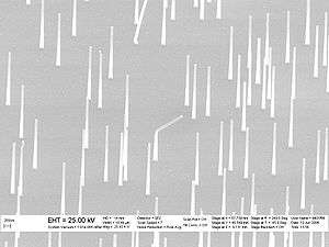
There are two basic approaches to synthesizing nanowires: top-down and bottom-up. A top-down approach reduces a large piece of material to small pieces, by various means such as lithography,[5][6] milling or thermal oxidation. A bottom-up approach synthesizes the nanowire by combining constituent adatoms. Most synthesis techniques use a bottom-up approach. Initial synthesis via either method may often be followed by a nanowire thermal treatment step, often involving a form of self-limiting oxidation, to fine tune the size and aspect ratio of the structures.[7]
Nanowire production uses several common laboratory techniques, including suspension, electrochemical deposition, vapor deposition, and VLS growth. Ion track technology enables growing homogeneous and segmented nanowires down to 8 nm diameter. As nanowire oxidation rate is controlled by diameter, thermal oxidation steps are often applied to tune their morphology.
Suspension
A suspended nanowire is a wire produced in a high-vacuum chamber held at the longitudinal extremities. Suspended nanowires can be produced by:
- The chemical etching of a larger wire
- The bombardment of a larger wire, typically with highly energetic ions
- Indenting the tip of a STM in the surface of a metal near its melting point, and then retracting it
VLS growth
A common technique for creating a nanowire is vapor-liquid-solid method (VLS), which was first reported by Wagner and Ellis in 1964 for silicon whiskers with diameters ranging from hundreds of nm to hundreds of µm.[8] This process can produce high-quality crystalline nanowires of many semiconductor materials, for example, VLS–grown single crystalline silicon nanowires (SiNWs) with smooth surfaces could have excellent properties, such as ultra-large elasticity.[9] This method uses a source material from either laser ablated particles or a feed gas such as silane.
VLS synthesis requires a catalyst. For nanowires, the best catalysts are liquid metal (such as gold) nanoclusters, which can either be self-assembled from a thin film by dewetting, or purchased in colloidal form and deposited on a substrate.
The source enters these nanoclusters and begins to saturate them. On reaching supersaturation, the source solidifies and grows outward from the nanocluster. Simply turning off the source can adjust the final length of the nanowire. Switching sources while still in the growth phase can create compound nanowires with super-lattices of alternating materials.
A single-step vapour phase reaction at elevated temperature synthesises inorganic nanowires such as Mo6S9−xIx. From another point of view, such nanowires are cluster polymers.
VSS Growth Similar to VLS synthesis, VSS (vapor-solid-solid) synthesis of nanowires (NWs) proceeds through thermolytic decomposition of a silicon precursor (typically phenylsilane). Unlike VLS, the catalytic seed remains in solid state when subjected to high temperature annealing of the substrate. This such type of synthesis is widely used to synthesise metal silicide/germanide nanowires through VSS alloying between a copper substrate and a silicon/germanium precursor.
Solution-phase synthesis
Solution-phase synthesis refers to techniques that grow nanowires in solution. They can produce nanowires of many types of materials. Solution-phase synthesis has the advantage that it can produce very large quantities, compared to other methods. In one technique, the polyol synthesis, ethylene glycol is both solvent and reducing agent. This technique is particularly versatile at producing nanowires of gold,[10] lead, platinum, and silver.
The supercritical fluid-liquid-solid growth method[11][12] can be used to synthesize semiconductor nanowires, e.g., Si and Ge. By using metal nanocrystals as seeds,[13] Si and Ge organometallic precursors are fed into a reactor filled with a supercritical organic solvent, such as toluene. Thermolysis results in degradation of the precursor, allowing release of Si or Ge, and dissolution into the metal nanocrystals. As more of the semiconductor solute is added from the supercritical phase (due to a concentration gradient), a solid crystallite precipitates, and a nanowire grows uniaxially from the nanocrystal seed.
Non-catalytic growth
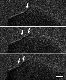
Nanowires can be also grown without the help of catalysts, which gives an advantage of pure nanowires and minimizes the number of technological steps. The simplest methods to obtain metal oxide nanowires use ordinary heating of the metals, e.g. metal wire heated with battery, by Joule heating in air[14] can be easily done at home. The vast majority of nanowire-formation mechanisms are explained through the use of catalytic nanoparticles, which drive the nanowire growth and are either added intentionally or generated during the growth. However the mechanisms for catalyst-free growth of nanowires (or whiskers) were known from 1950s.[15] Spontaneous nanowire formation by non-catalytic methods were explained by the dislocation present in specific directions[16][17] or the growth anisotropy of various crystal faces. More recently, after microscopy advancement, the nanowire growth driven by screw dislocations[18][19] or twin boundaries[20] were demonstrated. The picture on the right shows a single atomic layer growth on the tip of CuO nanowire, observed by in situ TEM microscopy during the non-catalytic synthesis of nanowire.
DNA-templated metallic nanowire synthesis
An emerging field is to use DNA strands as scaffolds for metallic nanowire synthesis. This method is investigated both for the synthesis of metallic nanowires in electronic components and for biosensing applications, in which they allow the transduction of a DNA strand into a metallic nanowire that can be electrically detected. Typically, ssDNA strands are stretched, whereafter they are decorated with metallic nanoparticles that have been functionalised with short complementary ssDNA strands.[21][22][23][24]
Physics
Conductivity of nanowires
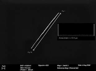
Several physical reasons predict that the conductivity of a nanowire will be much less than that of the corresponding bulk material. First, there is scattering from the wire boundaries, whose effect will be very significant whenever the wire width is below the free electron mean free path of the bulk material. In copper, for example, the mean free path is 40 nm. Copper nanowires less than 40 nm wide will shorten the mean free path to the wire width.
Nanowires also show other peculiar electrical properties due to their size. Unlike single wall carbon nanotubes, whose motion of electrons can fall under the regime of ballistic transport (meaning the electrons can travel freely from one electrode to the other), nanowire conductivity is strongly influenced by edge effects. The edge effects come from atoms that lay at the nanowire surface and are not fully bonded to neighboring atoms like the atoms within the bulk of the nanowire. The unbonded atoms are often a source of defects within the nanowire, and may cause the nanowire to conduct electricity more poorly than the bulk material. As a nanowire shrinks in size, the surface atoms become more numerous compared to the atoms within the nanowire, and edge effects become more important.
Furthermore, the conductivity can undergo a quantization in energy: i.e. the energy of the electrons going through a nanowire can assume only discrete values, which are multiples of the conductance quantum G = 2e2/h (where e is the charge of the electron and h is the Planck constant. See also the Quantum Hall effect).
The conductivity is hence described as the sum of the transport by separate channels of different quantized energy levels. The thinner the wire is, the smaller the number of channels available to the transport of electrons.
This quantization has been demonstrated by measuring the conductivity of a nanowire suspended between two electrodes while pulling it: as its diameter reduces, its conductivity decreases in a stepwise fashion and the plateaus correspond to multiples of G.
The quantization of conductivity is more pronounced in semiconductors like Si or GaAs than in metals, due to their lower electron density and lower effective mass. It can be observed in 25 nm wide silicon fins, and results in increased threshold voltage. In practical terms, this means that a MOSFET with such nanoscale silicon fins, when used in digital applications, will need a higher gate (control) voltage to switch the transistor on.[25]
Welding nanowires
To incorporate nanowire technology into industrial applications, researchers in 2008 developed a method of welding nanowires together: a sacrificial metal nanowire is placed adjacent to the ends of the pieces to be joined (using the manipulators of a scanning electron microscope); then an electric current is applied, which fuses the wire ends. The technique fuses wires as small as 10 nm.[26]
For nanowires with diameters less than 10 nm, existing welding techniques, which require precise control of the heating mechanism and which may introduce the possibility of damage, will not be practical. Recently scientists discovered that single-crystalline ultrathin gold nanowires with diameters ~3–10 nm can be "cold-welded" together within seconds by mechanical contact alone, and under remarkably low applied pressures (unlike macro- and micro-scale cold welding process).[27] High-resolution transmission electron microscopy and in situ measurements reveal that the welds are nearly perfect, with the same crystal orientation, strength and electrical conductivity as the rest of the nanowire. The high quality of the welds is attributed to the nanoscale sample dimensions, oriented-attachment mechanisms and mechanically assisted fast surface diffusion. Nanowire welds were also demonstrated between gold and silver, and silver nanowires (with diameters ~5–15 nm) at near room temperature, indicating that this technique may be generally applicable for ultrathin metallic nanowires. Combined with other nano- and microfabrication technologies,[28][29] cold welding is anticipated to have potential applications in the future bottom-up assembly of metallic one-dimensional nanostructures.
Mechanical properties of nanowires
Investigation of mechanical properties of nanowires
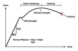
The study of nanowire mechanics has boomed since the advent of the Atomic Force Microscope (AFM), and associated technologies which have enabled direct study of the response of the nanowire to an applied load.[30] Specifically, a nanowire can be clamped from one end, and the free end displaced by an AFM tip. In this cantilever geometry, the height of the AFM is precisely known, and the force applied is precisely known. This allows for construction of a force vs. displacement curve, which can be converted to a stress vs. strain curve if the nanowire dimensions are known. From the stress-strain curve, the elastic constant known as the Young’s Modulus can be derived, as well as the toughness, and degree of strain-hardening.
Young's modulus of nanowires
The elastic component of the stress-strain curve described by the Young’s Modulus, has been reported for nanowires, however the modulus depends very strongly on the microstructure. Thus a complete description of the modulus dependence on diameter is lacking. Analytically, continuum mechanics has been applied to estimate the dependence of modulus on diameter: in tension, where is the bulk modulus, is the thickness of a shell layer in which the modulus is surface dependent and varies from the bulk, is the surface modulus, and is the diameter.[30] This equation implies that the modulus increases as the diameter decreases. However, various computational methods such as molecular dynamics have predicted that modulus should decrease as diameter decreases.
Experimentally, gold nanowires have been shown to have a Young’s modulus which is effectively diameter independent.[31] Similarly, nano-indentation was applied to study the modulus of silver nanowires, and again the modulus was found to be 88 GPa, very similar to the modulus of bulk Silver (85 GPa)[32] These works demonstrated that the analytically determined modulus dependence seems to be suppressed in nanowire samples where the crystalline structure highly resembles that of the bulk system.
In contrast, Si solid nanowires have been studied, and shown to have a decreasing modulus with diameter[33] The authors of that work report a Si modulus which is half that of the bulk value, and they suggest that the density of point defects, and or loss of chemical stoichiometry may account for this difference.
Yield strength of nanowires
The plastic component of the stress strain curve (or more accurately the onset of plasticity) is described by the yield strength. The strength of a material is increased by decreasing the number of defects in the solid, which occurs naturally in nanomaterials where the volume of the solid is reduced. As a nanowire is shrunk to a single line of atoms, the strength should theoretically increase all the way to the molecular tensile strength.[30] Gold nanowires have been described as ‘ultrahigh strength’ due to the extreme increase in yield strength, approaching the theoretical value of E/10.[31] This huge increase in yield is determined to be due to the lack of dislocations in the solid. Without dislocation motion, a ‘dislocation-starvation’ mechanism is in operation. The material can accordingly experience huge stresses before dislocation motion is possible, and then begins to strain-harden. For these reasons, nanowires (historically described as 'whiskers') have been used extensively in composites for increasing the overall strength of a material.[30] Moreover, nanowires continue to be actively studied, with research aiming to translate enhanced mechanical properties to novel devices in the fields of MEMS or NEMS.
Applications
Electronic devices
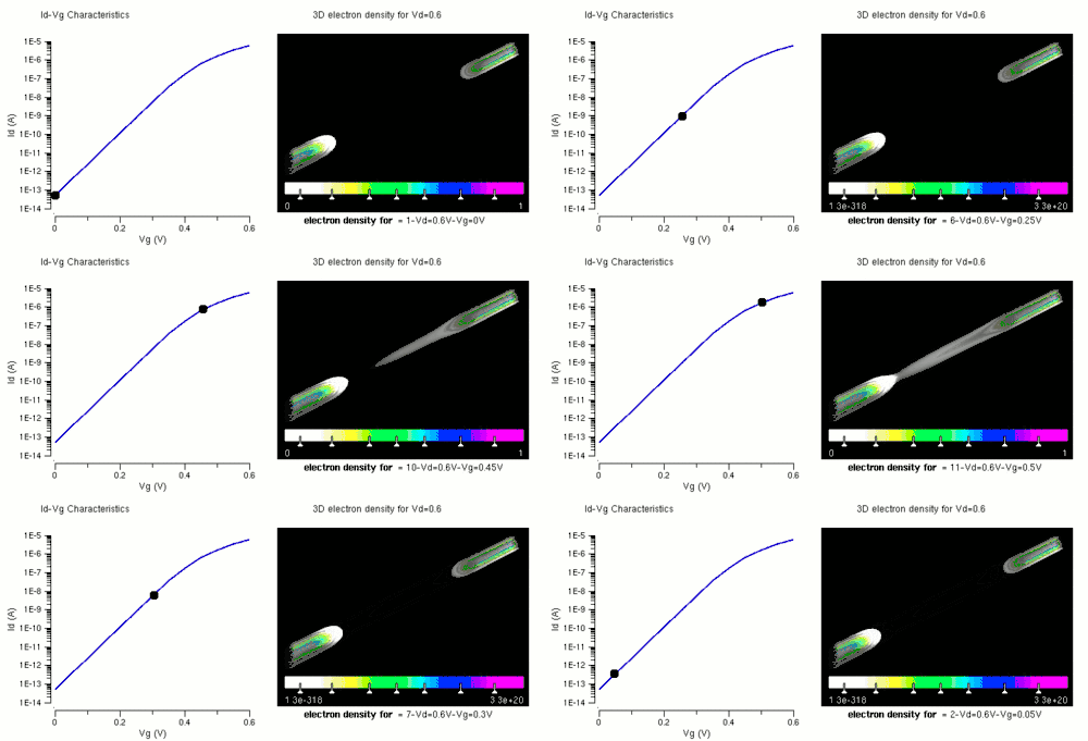
Nanowires can be used for MOSFETs (MOS field-effect transistors). MOS transistors are used widely as fundamental building elements in today's electronic circuits.[34][35] As predicted by Moore's law, the dimension of MOS transistors is shrinking smaller and smaller into nanoscale. One of the key challenges of building future nanoscale MOS transistors is ensuring good gate control over the channel. Due to the high aspect ratio, if the gate dielectric is wrapped around the nanowire channel, we can get good control of channel electrostatic potential, thereby turning the transistor on and off efficiently.
Due to the unique one-dimensional structure with remarkable optical properties, the nanowire also opens new opportunities for realizing high efficiency photovoltaic devices.[36] Compared with its bulk counterparts, the nanowire solar cells are less sensitive to impurities due to bulk recombination, and thus silicon wafers with lower purity can be used to achieve acceptable efficiency, leading to the a reduction on material consumption.[37]
To create active electronic elements, the first key step was to chemically dope a semiconductor nanowire. This has already been done to individual nanowires to create p-type and n-type semiconductors.
The next step was to find a way to create a p–n junction, one of the simplest electronic devices. This was achieved in two ways. The first way was to physically cross a p-type wire over an n-type wire. The second method involved chemically doping a single wire with different dopants along the length. This method created a p-n junction with only one wire.
After p-n junctions were built with nanowires, the next logical step was to build logic gates. By connecting several p-n junctions together, researchers have been able to create the basis of all logic circuits: the AND, OR, and NOT gates have all been built from semiconductor nanowire crossings.
In August 2012, researchers reported constructing the first NAND gate from undoped silicon nanowires. This avoids the problem of how to achieve precision doping of complementary nanocircuits, which is unsolved. They were able to control the Schottky barrier to achieve low-resistance contacts by placing a silicide layer in the metal-silicon interface.[38]
It is possible that semiconductor nanowire crossings will be important to the future of digital computing. Though there are other uses for nanowires beyond these, the only ones that actually take advantage of physics in the nanometer regime are electronic.[39]
In addition, nanowires are also being studied for use as photon ballistic waveguides as interconnects in quantum dot/quantum effect well photon logic arrays. Photons travel inside the tube, electrons travel on the outside shell.
When two nanowires acting as photon waveguides cross each other the juncture acts as a quantum dot.
Conducting nanowires offer the possibility of connecting molecular-scale entities in a molecular computer. Dispersions of conducting nanowires in different polymers are being investigated for use as transparent electrodes for flexible flat-screen displays.
Because of their high Young's moduli, their use in mechanically enhancing composites is being investigated. Because nanowires appear in bundles, they may be used as tribological additives to improve friction characteristics and reliability of electronic transducers and actuators.
Because of their high aspect ratio, nanowires are also uniquely suited to dielectrophoretic manipulation,[40][41][42] which offers a low-cost, bottom-up approach to integrating suspended dielectric metal oxide nanowires in electronic devices such as UV, water vapor, and ethanol sensors.[43]
Nanowire lasers
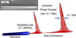
Nanowire lasers are nano-scaled lasers with potential as optical interconnects and optical data communication on chip. Nanowire lasers are built from III–V semiconductor heterostructures, the high refractive index allows for low optical loss in the nanowire core. Nanowire lasers are subwavelength lasers of only a few hundred nanometers.[44][45] Nanowire lasers are Fabry–Perot resonator cavities defined by the end facets of the wire with high-reflectivity, recent developments have demonstrated repetition rates greater than 200 GHz offering possibilities for optical chip level communications.[46][47]
Sensing of proteins and chemicals using semiconductor nanowires
In an analogous way to FET devices in which the modulation of conductance (flow of electrons/holes) in the semiconductor, between the input (source) and the output (drain) terminals, is controlled by electrostatic potential variation (gate-electrode) of the charge carriers in the device conduction channel, the methodology of a Bio/Chem-FET is based on the detection of the local change in charge density, or so-called “field effect”, that characterizes the recognition event between a target molecule and the surface receptor.
This change in the surface potential influences the Chem-FET device exactly as a ‘gate’ voltage does, leading to a detectable and measurable change in the device conduction. When these devices are fabricated using semiconductor nanowires as the transistor element the binding of a chemical or biological species to the surface of the sensor can lead to the depletion or accumulation of charge carriers in the "bulk" of the nanometer diameter nanowire i.e. (small cross section available for conduction channels). Moreover, the wire, which serves as a tunable conducting channel, is in close contact with the sensing environment of the target, leading to a short response time, along with orders of magnitude increase in the sensitivity of the device as a result of the huge S/V ratio of the nanowires.
While several inorganic semiconducting materials such as Si, Ge, and metal oxides (e.g. In2O3, SnO2, ZnO, etc.) have been used for the preparation of nanowires, Si is usually the material of choice when fabricating nanowire FET-based chemo/biosensors.[48]
Several examples of the use of silicon nanowire(SiNW) sensing devices include the ultra sensitive, real-time sensing of biomarker proteins for cancer, detection of single virus particles, and the detection of nitro-aromatic explosive materials such as 2,4,6 Tri-nitrotoluene (TNT) in sensitives superior to these of canines.[49] Silicon nanowires could also be used in their twisted form, as electromechanical devices, to measure intermolecular forces with great precision.[50]
Limitations of sensing with silicon nanowire FET devices
Generally, the charges on dissolved molecules and macromolecules are screened by dissolved counterions, since in most cases molecules bound to the devices are separated from the sensor surface by approximately 2–12 nm (the size of the receptor proteins or DNA linkers bound to the sensor surface). As a result of the screening, the electrostatic potential that arises from charges on the analyte molecule decays exponentially toward zero with distance. Thus, for optimal sensing, the Debye length must be carefully selected for nanowire FET measurements. One approach of overcoming this limitation employs fragmentation of the antibody-capturing units and control over surface receptor density, allowing more intimate binding to the nanowire of the target protein. This approach proved useful for dramatically enhancing the sensitivity of cardiac biomarkers (e.g. Troponin) detection directly from serum for the diagnosis of acute myocardial infarction.[51]
Corn-like nanowires
Corn-like nanowire is a one-dimensional nanowire with interconnected nanoparticles on the surface, providing a large percentage of reactive facets. TiO2 corn-like nanowires were first prepared by a surface modification concept using surface tension stress mechanism through a two consecutive hydrothermal operation, and showed an increase of 12% in dye-sensitized solar cell efficiency the light scattering layer.[52] CdSe corn-like nanowires grown by chemical bath deposition and corn-like γ-Fe2O3@SiO2@TiO2 photocatalysts induced by magnetic dipole interactions have been also reported previously.[53][54]
See also
- Bacterial nanowires
- Inorganic nanotubes
- Molecular nanowires
- Nanoantenna
- Nanorods
- Nanowire battery
- Silicon nanowires
- Solar cell
References
- Boston, R.; Schnepp, Z.; Nemoto, Y.; Sakka, Y.; Hall, S. R. (2014). "In Situ TEM Observation of a Microcrucible Mechanism of Nanowire Growth". Science. 344 (6184): 623–6. Bibcode:2014Sci...344..623B. doi:10.1126/science.1251594. hdl:1983/8f23c618-23f8-46e1-a1d9-960a0b491b1f. PMID 24812400. S2CID 206555658.
- Carter, Robin; Suyetin, Mikhail; Lister, Samantha; Dyson, M. Adam; Trewhitt, Harrison; Goel, Sanam; Liu, Zheng; Suenaga, Kazu; Giusca, Cristina; Kashtiban, Reza J.; Hutchison, John L.; Dore, John C.; Bell, Gavin R.; Bichoutskaia, Elena; Sloan, Jeremy (2014). "Band gap expansion, shear inversion phase change behaviour and low-voltage induced crystal oscillation in low-dimensional tin selenide crystals". Dalton Trans. 43 (20): 7391–9. doi:10.1039/C4DT00185K. PMID 24637546.
- Spencer, Joseph; Nesbitt, John; Trewhitt, Harrison; Kashtiban, Reza; Bell, Gavin; Ivanov, Victor; Faulques, Eric; Smith, David (2014). "Raman Spectroscopy of Optical Transitions and Vibrational Energies of ~1 nm HgTe Extreme Nanowires within Single Walled Carbon Nanotubes" (PDF). ACS Nano. 8 (9): 9044–52. doi:10.1021/nn5023632. PMID 25163005.
- von Klitzing constant. physics.nist.gov
- Shkondin, E.; Takayama, O., Aryaee Panah, M. E.; Liu, P., Larsen, P. V.; Mar, M. D., Jensen, F.; Lavrinenko, A. V. (2017). "Large-scale high aspect ratio Al-doped ZnO nanopillars arrays as anisotropic metamaterials" (PDF). Optical Materials Express. 7 (5): 1606–1627. Bibcode:2017OMExp...7.1606S. doi:10.1364/OME.7.001606.
- Shkondin, E.; Alimadadi, H., Takayama, O.; Jensen, F., Lavrinenko, A. V. (2020). "Fabrication of hollow coaxial Al2O3/ZnAl2O4 high aspect ratio freestanding nanotubes based on the Kirkendall effect". Journal of Vacuum Science & Technology A. 38 (1): 1606–1627. Bibcode:2020JVSTA..38a3402S. doi:10.1116/1.5130176.
- Liu, M.; Peng, J.; et al. (2016). "Two-dimensional modeling of the self-limiting oxidation in silicon and tungsten nanowires". Theoretical and Applied Mechanics Letters. 6 (5): 195–199. doi:10.1016/j.taml.2016.08.002.
- Wagner, R. S.; Ellis, W. C. (1964). "Vapor-liquid-solid mechanism of single crystal growth". Appl. Phys. Lett. 4 (5): 89. Bibcode:1964ApPhL...4...89W. doi:10.1063/1.1753975.
- Zhang, H.; et al. (2016). "Approaching the ideal elastic strain limit in silicon nanowires". Science Advances. 2 (8): e1501382. Bibcode:2016SciA....2E1382Z. doi:10.1126/sciadv.1501382. PMC 4988777. PMID 27540586.
- Yin, Xi; Wu, Jianbo; Li, Panpan; Shi, Miao; Yang, Hong (January 2016). "Self-Heating Approach to the Fast Production of Uniform Metal Nanostructures". ChemNanoMat. 2 (1): 37–41. doi:10.1002/cnma.201500123.
- Holmes, J. D.; Johnston, K. P.; Doty, R. C.; Korgel, B. A. (2000). "Control of thickness and orientation of solution-grown silicon nanowires". Science. 287 (5457): 1471–3. Bibcode:2000Sci...287.1471H. doi:10.1126/science.287.5457.1471. PMID 10688792.
- Heitsch, Andrew T.; Akhavan, Vahid A.; Korgel, Brian A. (2011). "Rapid SFLS Synthesis of Si Nanowires Using Trisilane with in situ Alkyl-Amine Passivation". Chemistry of Materials. 23 (11): 2697–2699. doi:10.1021/cm2007704.
- Hanrath, T.; Korgel, B.A. (2003). "Supercritical Fluid–Liquid–Solid (SFLS) Synthesis of Si and Ge Nanowires Seeded by Colloidal Metal Nanocrystals". Advanced Materials. 15 (5): 437–440. doi:10.1002/adma.200390101.
- Rackauskas, S.; Nasibulin, A. G.; Jiang, H.; Tian, Y.; Kleshch, V. I.; Sainio, J.; Obraztsova, E. D.; Bokova, S. N.; Obraztsov, A. N.; Kauppinen, E. I. (2010). "A Novel Method for Metal Oxide Nanowire Synthesis". Nanotechnology. 20 (16): 165603. Bibcode:2009Nanot..20p5603R. doi:10.1088/0957-4484/20/16/165603. PMID 19420573. S2CID 3529748.
- Sears, G.W. (1955). "A Growth Mechanism for Mercury Whiskers". Acta Metall. 3 (4): 361–366. doi:10.1016/0001-6160(55)90041-9.
- Frank, F. C. (1949). "The influence of dislocations on crystal growth". Discussions of the Faraday Society. 5: 48. doi:10.1039/df9490500048. S2CID 53512926.
- Burton, W. K.; Cabrera, N.; Frank, F. C. (1951). "The Growth of Crystals and the Equilibrium Structure of Their Surfaces". Philos. Trans. R. Soc. London A. 243 (866): 299–358. Bibcode:1951RSPTA.243..299B. doi:10.1098/rsta.1951.0006. S2CID 119643095.
- Morin, S. A.; Bierman, M. J.; Tong, J.; Jin, S. (2010). "Mechanism and Kinetics of Spontaneous Nanotube Growth Driven by Screw Dislocations". Science. 328 (5977): 476–480. Bibcode:2010Sci...328..476M. doi:10.1126/science.1182977. PMID 20413496. S2CID 30955349.
- Bierman, M. J.; Lau, Y. K. A.; Kvit, A. V; Schmitt, A. L.; Jin, S. (2008). "Dislocation-Driven Nanowire Growth and Eshelby Twist". Science. 320 (5879): 1060–1063. Bibcode:2008Sci...320.1060B. doi:10.1126/science.1157131. PMID 18451264. S2CID 20919593.
- Rackauskas, S.; Jiang, H.; Wagner, J. B.; Shandakov, S. D.; Hansen, T. W.; Kauppinen, E. I.; Nasibulin, A. G. (2014). "In Situ Study of Noncatalytic Metal Oxide Nanowire Growth". Nano Lett. 14 (10): 5810–5813. Bibcode:2014NanoL..14.5810R. doi:10.1021/nl502687s. PMID 25233273.
- Guo; et al. (2018). "Efficient DNA-assisted synthesis of trans-membrane gold nanowires". Microsystems & Nanoengineering. 4: 17084. doi:10.1038/micronano.2017.84.
- Teschome, Bezu; Facsko, Stefan; Schönherr, Tommy; Kerbusch, Jochen; Keller, Adrian; Erbe, Artur (2016). "Temperature-Dependent Charge Transport through Individually Contacted DNA Origami-Based Au Nanowires". Langmuir. 32 (40): 10159–10165. doi:10.1021/acs.langmuir.6b01961. PMID 27626925.
- Rakitin, A; Aich, P; Papadopoulos, C; Kobzar, Yu; Vedeneev, A. S; Lee, J. S; Xu, J. M (2001). "Metallic Conduction through Engineered DNA: DNA Nanoelectronic Building Blocks". Physical Review Letters. 86 (16): 3670–3. Bibcode:2001PhRvL..86.3670R. doi:10.1103/PhysRevLett.86.3670. PMID 11328050.
- Ongaro, A; Griffin, F; Nagle, L; Iacopino, D; Eritja, R; Fitzmaurice, D (2004). "DNA-Templated Assembly of a Protein-Functionalized Nanogap Electrode". Advanced Materials. 16 (20): 1799–1803. doi:10.1002/adma.200400244.
- Tilke, A. T.; Simmel, F. C.; Lorenz, H.; Blick, R. H.; Kotthaus, J. P. (2003). "Quantum interference in a one-dimensional silicon nanowire". Physical Review B. 68 (7): 075311. Bibcode:2003PhRvB..68g5311T. doi:10.1103/PhysRevB.68.075311.
- Halford, Bethany (2008). "Wee Welding with Nanosolder". Chemical & Engineering News. 86 (51): 35.
- Lu, Yang; Huang, Jian Yu; Wang, Chao; Sun, Shouheng; Lou, Jun (2010). "Cold welding of ultrathin gold nanowires". Nature Nanotechnology. 5 (3): 218–24. Bibcode:2010NatNa...5..218L. doi:10.1038/nnano.2010.4. PMID 20154688.
- Zhong, Z.; Wang, D; Cui, Y; Bockrath, M. W.; Lieber, C. M. (2003). "Nanowire Crossbar Arrays as Address Decoders for Integrated Nanosystems" (PDF). Science. 302 (5649): 1377–9. Bibcode:2003Sci...302.1377Z. doi:10.1126/science.1090899. PMID 14631034. S2CID 35084433.
- Huo, F.; Zheng, Z.; Zheng, G.; Giam, L. R.; Zhang, H.; Mirkin, C. A. (2008). "Polymer Pen Lithography" (PDF). Science. 321 (5896): 1658–60. Bibcode:2008Sci...321.1658H. doi:10.1126/science.1162193. PMID 18703709. S2CID 354452.
- Wang, Shiliang; Shan, Zhiwei; Huang, Han (2017-01-03). "The Mechanical Properties of Nanowires". Advanced Science. 4 (4): 1600332. doi:10.1002/advs.201600332. PMC 5396167. PMID 28435775.
- Wu, Bin; Heidelberg, Andreas; Boland, John J. (2005-06-05). "Mechanical properties of ultrahigh-strength gold nanowires". Nature Materials. 4 (7): 525–529. Bibcode:2005NatMa...4..525W. doi:10.1038/nmat1403. ISSN 1476-1122. PMID 15937490. S2CID 34828518.
- Li, Xiaodong; Gao, Hongsheng; Murphy, Catherine J.; Caswell, K. K. (Nov 2003). "Nanoindentation of Silver Nanowires". Nano Letters. 3 (11): 1495–1498. Bibcode:2003NanoL...3.1495L. doi:10.1021/nl034525b. ISSN 1530-6984.
- Wang, Zhong Lin; Dai, Zu Rong; Gao, Ruiping; Gole, James L. (2002-03-27). "Measuring the Young's modulus of solid nanowires byin situTEM". Journal of Electron Microscopy. 51 (suppl 1): S79–S85. doi:10.1093/jmicro/51.Supplement.S79. ISSN 0022-0744. S2CID 53588258.
- "Triumph of the MOS Transistor". YouTube. Computer History Museum. 6 August 2010. Retrieved 21 July 2019.
- Raymer, Michael G. (2009). The Silicon Web: Physics for the Internet Age. CRC Press. p. 365. ISBN 9781439803127.
- Yu, Peng; Wu, Jiang; Liu, Shenting; Xiong, Jie; Jagadish, Chennupati; Wang, Zhiming M. (2016-12-01). "Design and fabrication of silicon nanowires towards efficient solar cells". Nano Today. 11 (6): 704–737. doi:10.1016/j.nantod.2016.10.001.
- Kayes, Brendan M.; Atwater, Harry A.; Lewis, Nathan S. (2005-05-23). "Comparison of the device physics principles of planar and radial p-n junction nanorod solar cells" (PDF). Journal of Applied Physics. 97 (11): 114302–114302–11. Bibcode:2005JAP....97k4302K. doi:10.1063/1.1901835. ISSN 0021-8979.
- Mongillo, Massimo; Spathis, Panayotis; Katsaros, Georgios; Gentile, Pascal; De Franceschi, Silvano (2012). "Multifunctional Devices and Logic Gates with Undoped Silicon Nanowires". Nano Letters. 12 (6): 3074–9. arXiv:1208.1465. Bibcode:2012NanoL..12.3074M. doi:10.1021/nl300930m. PMID 22594644. S2CID 22112655.
- Appenzeller, Joerg; Knoch, Joachim; Bjork, Mikael T.; Riel, Heike; Schmid, Heinz; Riess, Walter (2008). "Toward nanowire electronics". IEEE Transactions on Electron Devices. 55 (11): 2827–2845. Bibcode:2008ITED...55.2827A. doi:10.1109/TED.2008.2008011. S2CID 703393.
- Wissner-Gross, A. D. (2006). "Dielectrophoretic reconfiguration of nanowire interconnects" (PDF). Nanotechnology. 17 (19): 4986–4990. Bibcode:2006Nanot..17.4986W. doi:10.1088/0957-4484/17/19/035.
- "Nanowires get reconfigured". nanotechweb.org. October 19, 2006. Archived from the original on May 22, 2007. Retrieved January 18, 2007.
- Grange, R.; Choi, J.W.; Hsieh, C.L.; Pu, Y.; Magrez, A.; Smajda, R.; Forro, L.; Psaltis, D. (2009). "Lithium niobate nanowires: synthesis, optical properties and manipulation". Applied Physics Letters. 95 (14): 143105. Bibcode:2009ApPhL..95n3105G. doi:10.1063/1.3236777. Archived from the original on 2016-05-14.
- Vizcaíno, J. L. P.; Núñez, C. G. A. (2013). "Fast, effective manipulation of nanowires for electronic devices". SPIE Newsroom. doi:10.1117/2.1201312.005260. S2CID 124474608.
- Koblmüller, Gregor; et al. (2017). "GaAs–AlGaAs core–shell nanowire lasers on silicon: invited review". Semiconductor Science and Technology. 32 (5). 053001. Bibcode:2017SeScT..32e3001K. doi:10.1088/1361-6641/aa5e45.
- Yan, Ruoxue; Gargas, Daniel; Yang, Peidong (2009). "Nanowire photonics". Nature Photonics. 3 (10): 569–576. Bibcode:2009NaPho...3..569Y. doi:10.1038/nphoton.2009.184.
- Mayer, B.; et al. (2015). "Monolithically integrated high-β nanowire lasers on silicon". Nano Letters. 16 (1): 152–156. doi:10.1021/acs.nanolett.5b03404.
- Mayer, B.; et al. (2017). "Long-term mutual phase locking of picosecond pulse pairs generated by a semiconductor nanowire laser". Nature Communications. 8. 15521. arXiv:1603.02169. Bibcode:2017NatCo...815521M. doi:10.1038/ncomms15521. PMID 28534489. S2CID 1099474.
- Lu, Wei; Xiang, Jie, eds. (2015). Semiconductor Nanowires. Cambridge: Royal Society of Chemistry.
- Engel, Yoni; Elnathan, Roey; Pevzner, Alexander; Davidi, Guy; Flaxer, Eli; Patolsky, Fernando (2010). "Supersensitive Detection of Explosives by Silicon Nanowire Arrays". Angewandte Chemie International Edition. 49 (38): 6830–6835. doi:10.1002/anie.201000847. PMID 20715224.
- Garcia, J. C.; Justo, J. F. (2014). "Twisted ultrathin silicon nanowires: A possible torsion electromechanical nanodevice". Europhys. Lett. 108 (3): 36006. arXiv:1411.0375. Bibcode:2014EL....10836006G. doi:10.1209/0295-5075/108/36006. S2CID 118792981.
- Elnathan, Roey; Kwiat, M.; Pevzner, A.; Engel, Y.; Burstein, L.; Khatchtourints, A.; Lichtenstein, A.; Kantaev, R.; Patolsky, F. (10 September 2012). "Biorecognition Layer Engineering: Overcoming Screening Limitations of Nanowire-Based FET Devices". Nano Letters. 12 (10): 5245–5254. Bibcode:2012NanoL..12.5245E. doi:10.1021/nl302434w. PMID 22963381.
- Bakhshayesh, A. M.; Mohammadi, M. R.; Dadar, H.; Fray, D. J. (2013). "Improved efficiency of dye-sensitized solar cells aided by corn-like TiO2 nanowires as the light scattering layer". Electrochimica Acta. 90 (15): 302–308. doi:10.1016/j.electacta.2012.12.065.
- Gubur, H. M.; Septekin, F.; Alpdogan, S.; Sahan, B.; Zeyrek, B. K. (2016). "Structural properties of CdSe corn-like nanowires grown by chemical bath deposition". Journal of Materials Science: Materials in Electronics. 27 (7): 7640–7645. doi:10.1007/s10854-016-4748-2. S2CID 137884561.
- Wang, F.; Li, M.; Yu, L.; Sun, F.; Wang, Z.; Zhang, L.; Zeng, H.; Xu, X. (2017). "Corn-like, Recoverable γ-Fe2O3@SiO2@TiO2 Photocatalyst Induced by Magnetic Dipole Interactions". Sci Rep. 7 (1). 6960. Bibcode:2017NatSR...7.6960W. doi:10.1038/s41598-017-07417-z. PMID 28761085. S2CID 6058050.
External links
| Look up nanowire in Wiktionary, the free dictionary. |
- Nanohedron.com | Nano Image Gallery several images of nanowires are included in the galleries.
- Stanford's nanowire battery holds 10 times the charge of existing ones
- Original article on the Quantum Hall Effect: K. v. Klitzing, G. Dorda, and M. Pepper; Phys. Rev. Lett. 45, 494–497 (1980).
- Strongest theoretical nanowire produced at Australia's University of Melbourne.
- Penn Engineers Design Electronic Computer Memory in Nanoscale Form That Retrieves Data 1,000 Times Faster.
- One atom thick, hundreds of nanometers long Pt-nanowires are one of the best examples of self-assembly. (University of Twente)