Dawon Kahng
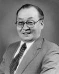
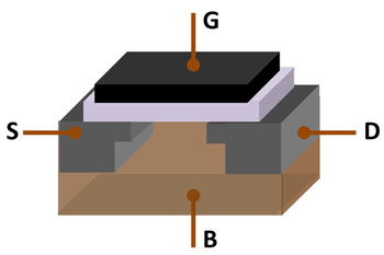
Dawon Kahng (May 4, 1931 – May 13, 1992) was a Korean-American electrical engineer and inventor, known for his work in solid-state electronics. He is best known for inventing the MOSFET (metal-oxide-semiconductor field-effect transistor), also known as the MOS transistor, with Mohamed Atalla in 1959. Atalla and Kahng developed both the PMOS and NMOS processes for MOSFET semiconductor device fabrication. The MOSFET is the most widely used type of transistor, and the basic element in most modern electronic equipment.
Dawon Kahng | |
|---|---|
강대원 | |
 | |
| Born | May 4, 1931[1] |
| Died | May 13, 1992 (aged 61) [2] |
| Nationality | South Korean (renounced) American |
| Occupation | Electrical engineer |
| Known for | MOSFET (MOS transistor) PMOS and NMOS Schottky diode Nanolayer-base transistor Floating-gate MOSFET Floating-gate memory Reprogrammable ROM |
Atalla and Kahng later proposed the concept of the MOS integrated circuit, and they did pioneering work on Schottky diodes and nanolayer-base transistors in the early 1960s. Kahng then invented the floating-gate MOSFET (FGMOS) with Simon Sze in 1967. Kahng and Sze proposed that FGMOS could be used as floating-gate memory cells for non-volatile memory (NVM) and reprogrammable read-only memory (ROM), which became the basis for EPROM (erasable programmable ROM), EEPROM (electrically erasable programmable ROM) and flash memory technologies. Kahng was inducted into the National Inventors Hall of Fame in 2009.
Biography
Dawon Kahng was born on May 4, 1931, in Seoul, Korea. He studied Physics at Seoul National University in South Korea, and immigrated to the United States in 1955 to attend Ohio State University, where he received a doctorate in physics.

He was a researcher at Bell Telephone Laboratories in Murray Hill, New Jersey, and he invented MOSFET (metal-oxide-semiconductor field-effect transistor), which is the basic element in most of today's electronic equipment, with Mohamed Atalla in 1959.[3] They fabricated both PMOS and NMOS devices with a 20 µm process.[4]
Atalla in 1960, and then Kahng in 1961, proposed the concept of the MOS integrated circuit. They noted that the MOS transistor's ease of fabrication made it useful for integrated circuits.[5][6] However, Bell Labs initially ignored MOS technology, as the company was not interested in integrated circuits at the time.[5]
Extending their work on MOS technology, Atalla and Kahng next did pioneering work on hot carrier devices, which used what would later be called a Schottky barrier.[7] The Schottky diode, also known as the Schottky-barrier diode, was theorized for years, but was first practically realized as a result of the work of Atalla and Kahng during 1960–1961.[8] They published their results in 1962 and called their device the "hot electron" triode structure with semiconductor-metal emitter.[9] The Schottky diode went on to assume a prominent role in mixer applications.[8] They later conducted further research on high-frequency Schottky diodes.
In 1962, Atalla and Kahng proposed and demonstrated an early metal nanolayer-base transistor. This device has a metallic layer with nanometric thickness sandwiched between two semiconducting layers, with the metal forming the base and the semiconductors forming the emitter and collector. With its low resistance and short transit times in the thin metallic nanolayer base, the device was capable of high operation frequency compared to bipolar transistors. Their pioneering work involved depositing metal layers (the base) on top of single crystal semiconductor substrates (the collector), with the emitter being a crystalline semiconductor piece with a top or a blunt corner pressed against the metallic layer (the point contact). They deposited gold (Au) thin films with a thickness of 10 nm on n-type germanium (n-Ge), while the point contact was n-type silicon (n-Si).[10]
Along with his colleague Simon Sze, he invented the floating-gate MOSFET, which they first reported in 1967.[11] They also invented the floating-gate memory cell, the foundation for many forms of semiconductor memory devices. He invented floating-gate non-volatile memory in 1967, and proposed that the floating gate of an MOS semiconductor device could be used for the cell of a reprogrammable ROM, which became the basis for EPROM (erasable programmable ROM),[12] EEPROM (electrically erasable programmable ROM) and flash memory technologies. He also conducted research on ferro-electric semiconductors and luminous materials, and made important contributions to the field of electroluminescence.
After retiring from Bell Laboratories, he became the founding president of the NEC Research Institute in New Jersey. He was a fellow of the IEEE and a fellow of the Bell Laboratories. He was also a recipient of the Stuart Ballantine Medal of the Franklin Institute and the Distinguished Alumnus Award of the Ohio State University College of Engineering. He died of complications following emergency surgery for a ruptured aortic aneurysm in 1992.[13]
Awards and honors
Kahng and Mohamed Atalla were awarded the Stuart Ballantine Medal at the 1975 Franklin Institute Awards, for their invention of the MOSFET.[14][15] In 2009, Kahng was inducted into the National Inventors Hall of Fame.[16] In 2014, the 1959 invention of the MOSFET was included on the list of IEEE milestones in electronics.[17]
Despite the MOSFET enabling Nobel Prize winning breakthroughs such as the quantum Hall effect[18] and the charge-coupled device (CCD),[19] there was never any Nobel Prize given for the MOSFET itself.[20] In 2018, the Royal Swedish Academy of Sciences which awards the science Nobel Prizes acknowledged that the invention of the MOSFET by Atalla and Kahng was one of the most important inventions in microelectronics and in information and communications technology (ICT).[21]
References
- "Dawon Kahng". National Inventors Hall of Fame. 2009. Archived from the original on 28 March 2009. Retrieved 28 March 2009.
- New York Times obituary
- "1960 - Metal Oxide Semiconductor (MOS) Transistor Demonstrated". Computer History Museum. Retrieved 11 November 2012.
- Lojek, Bo (2007). History of Semiconductor Engineering. Springer Science & Business Media. pp. 321-3. ISBN 9783540342588.
- Moskowitz, Sanford L. (2016). Advanced Materials Innovation: Managing Global Technology in the 21st century. John Wiley & Sons. pp. 165–167. ISBN 9780470508923.
- Bassett, Ross Knox (2007). To the Digital Age: Research Labs, Start-up Companies, and the Rise of MOS Technology. Johns Hopkins University Press. pp. 22–25. ISBN 9780801886393.
- Bassett, Ross Knox (2007). To the Digital Age: Research Labs, Start-up Companies, and the Rise of MOS Technology. Johns Hopkins University Press. p. 328. ISBN 9780801886393.
- The Industrial Reorganization Act: The communications industry. U.S. Government Printing Office. 1973. p. 1475.
- Atalla, M.; Kahng, D. (November 1962). "A new "Hot electron" triode structure with semiconductor-metal emitter". IRE Transactions on Electron Devices. 9 (6): 507–508. Bibcode:1962ITED....9..507A. doi:10.1109/T-ED.1962.15048. ISSN 0096-2430. S2CID 51637380.
- Pasa, André Avelino (2010). "Chapter 13: Metal Nanolayer-Base Transistor". Handbook of Nanophysics: Nanoelectronics and Nanophotonics. CRC Press. pp. 13–1, 13–4. ISBN 9781420075519.
- D. Kahng and S. M. Sze, "A floating-gate and its application to memory devices", The Bell System Technical Journal, vol. 46, no. 4, 1967, pp. 1288–1295
- "1971: Reusable semiconductor ROM introduced". Computer History Museum. Retrieved 19 June 2019.
- New York Times obituary
- Calhoun, Dave; Lustig, Lawrence K. (1976). 1977 Yearbook of science and the future. Encyclopaedia Britannica. p. 418. ISBN 9780852293195.
Three scientists were named recipients of the Franklin lnstitute's Stuart Ballantine Medal in 1975 [...] Martin M. Atalla, president of Atalla Technovations in California, and Dawon Kahng of Bell Laboratories were chosen "for their contributions to semiconductor silicon-silicon dioxide technology, and for the development of the MOS insulated gate, field-effect transistor.
- "Dawon Kahng". Franklin Institute Awards. The Franklin Institute. 14 January 2014. Retrieved 23 August 2019.
- "Dawon Kahng". National Inventors Hall of Fame. Retrieved 27 June 2019.
- "Milestones:List of IEEE Milestones". Institute of Electrical and Electronics Engineers. Retrieved 25 July 2019.
- Lindley, David (15 May 2015). "Focus: Landmarks—Accidental Discovery Leads to Calibration Standard". Physics. 8. doi:10.1103/Physics.8.46.
- Williams, J. B. (2017). The Electronics Revolution: Inventing the Future. Springer. pp. 245 & 249. ISBN 9783319490885.
- Woodall, Jerry M. (2010). Fundamentals of III-V Semiconductor MOSFETs. Springer Science & Business Media. p. 2. ISBN 9781441915474.
- "Advanced information on the Nobel Prize in Physics 2000" (PDF). Nobel Prize. June 2018. Retrieved 17 August 2019.