IA-64
IA-64 (also called Intel Itanium architecture) is the instruction set architecture (ISA) of the Itanium family of 64-bit Intel microprocessors. The basic ISA specification originated at Hewlett-Packard (HP), and was evolved and then implemented in a new processor microarchitecture by Intel with HP's continued partnership and expertise on the underlying EPIC design concepts. In order to establish what was their first new ISA in 20 years and bring an entirely new product line to market, Intel made a massive investment in product definition, design, software development tools, OS, software industry partnerships, and marketing. To support this effort Intel created the largest design team in their history and a new marketing and industry enabling team completely separate from x86. The first Itanium processor, codenamed Merced, was released in 2001.
| Designer | HP and Intel |
|---|---|
| Bits | 64-bit |
| Introduced | 2001 |
| Design | EPIC |
| Type | Register-Register |
| Encoding | Fixed |
| Branching | Condition register |
| Endianness | Selectable |
| Registers | |
| General purpose | 128 (64 bits plus 1 trap bit; 32 are static, 96 use register windows); 64 1-bit predicate registers |
| Floating point | 128 |

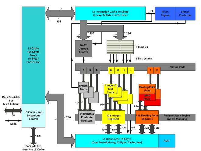
The Itanium architecture is based on explicit instruction-level parallelism, in which the compiler decides which instructions to execute in parallel. This contrasts with superscalar architectures, which depend on the processor to manage instruction dependencies at runtime. In all Itanium models, up to and including Tukwila, cores execute up to six instructions per clock cycle.
In 2008, Itanium was the fourth-most deployed microprocessor architecture for enterprise-class systems, behind x86-64, Power ISA, and SPARC.[1]
History
Development: 1989–2000
In 1989, HP began to become concerned that reduced instruction set computing (RISC) architectures were approaching a processing limit at one instruction per cycle. Both Intel and HP researchers had been exploring computer architecture options for future designs and separately began investigating a new concept known as very long instruction word (VLIW)[2] which came out of research by Yale University in the early 1980s.[3] VLIW is a computer architecture concept (like RISC and CISC) where a single instruction word contains multiple instructions encoded in one very long instruction word to facilitate the processor executing multiple instructions in each clock cycle. Typical VLIW implementations rely heavily on sophisticated compilers to determine at compile time which instructions can be executed at the same time and the proper scheduling of these instructions for execution and also to help predict the direction of branch operations. The value of this approach is to do more useful work in fewer clock cycles and to simplify processor instruction scheduling and branch prediction hardware requirements, with a penalty in increased processor complexity, cost, and energy consumption in exchange for faster execution.
Production
During this time, HP had begun to believe that it was no longer cost-effective for individual enterprise systems companies such as itself to develop proprietary microprocessors. Intel had also been researching several architectural options for going beyond the x86 ISA to address high end enterprise server and high performance computing (HPC) requirements. Thus Intel and HP partnered in 1994 to develop the IA-64 ISA, using a variation of VLIW design concepts which Intel named explicitly parallel instruction computing (EPIC). Intel's goal was to leverage the expertise HP had developed in their early VLIW work along with their own to develop a volume product line targeted at high-end enterprise class servers and high performance computing (HPC) systems that could be sold to all original equipment manufacturers (OEMs) while HP wished to be able to purchase off-the-shelf processors built using Intel's volume manufacturing and leading edge process technology that were higher performance and more cost effective than their current PA-RISC processors. Because the resulting products would be Intel's (HP would be one of many customers) and in order to achieve volumes necessary for a successful product line, the Itanium products would be required to meet the needs of the broader customer base and that software applications, OS, and development tools be available for these customers. This required that Itanium products be designed, documented, and manufactured, and have quality and support consistent with the rest of Intel's products. Therefore, Intel took the lead on microarchitecture design, productization (packaging, test, and all other steps), industry software and operating system enabling (Linux and Windows NT), and marketing. As part of Intel's definition and marketing process they engaged a wide variety of enterprise OEM's, software, and OS vendors, as well as end customers in order to understand their requirements and ensure they were reflected in the product family so as to meet the needs of a broad range of customers and end-users. HP made a substantial contribution to the ISA definition, the Merced/Itanium microarchitecture, and Itanium 2, but productization responsibility was Intel's. The original goal for delivering the first Itanium family product (codenamed Merced) was 1998.[2]
Marketing
Intel's product marketing and industry engagement efforts were substantial and achieved design wins with the majority of enterprise server OEM's including those based on RISC processors at the time, industry analysts predicted that IA-64 would dominate in servers, workstations, and high-end desktops, and eventually supplant RISC and complex instruction set computing (CISC) architectures for all general-purpose applications.[4][5] Compaq and Silicon Graphics decided to abandon further development of the Alpha and MIPS architectures respectively in favor of migrating to IA-64.[6]
By 1997, it was apparent that the IA-64 architecture and the compiler were much more difficult to implement than originally thought, and the delivery of Itanium began slipping.[7] Since Itanium was the first ever EPIC processor, the development effort encountered more unanticipated problems than the team was accustomed to. In addition, the EPIC concept depends on compiler capabilities that had never been implemented before, so more research was needed.[8]
Several groups developed operating systems for the architecture, including Microsoft Windows and Unix and Unix-like systems such as Linux, HP-UX, FreeBSD, Solaris,[9][10][11] Tru64 UNIX,[6] and Monterey/64[12] (the last three were canceled before reaching the market). In 1999, Intel led the formation of an open source industry consortium to port Linux to IA-64 they named "Trillium" (and later renamed "Trillian" due to a trademark issue) which was led by Intel and included Caldera Systems, CERN, Cygnus Solutions, Hewlett-Packard, IBM, Red Hat, SGI, SuSE, TurboLinux and VA Linux Systems. As a result, a working IA-64 Linux was delivered ahead of schedule and was the first OS to run on the new Itanium processors.
Intel announced the official name of the processor, Itanium, on October 4, 1999.[13] Within hours, the name Itanic had been coined on a Usenet newsgroup as a pun on the name Titanic, the "unsinkable" ocean liner that sank on its maiden voyage in 1912.[14]
Itanium (Merced): 2001
 Itanium processor | |
| General Info | |
|---|---|
| Launched | June 2001 |
| Discontinued | June 2002 |
| Common manufacturer(s) |
|
| Performance | |
| Max. CPU clock rate | 733 MHz to 800 MHz |
| FSB speeds | 266 MT/s |
| Cache | |
| L2 cache | 96 KB |
| L3 cache | 2 or 4 MB |
| Architecture and classification | |
| Instruction set | Itanium |
| Physical specifications | |
| Cores |
|
| Socket(s) | |
| Products, models, variants | |
| Core name(s) |
|
By the time Itanium was released in June 2001, its performance was not superior to competing RISC and CISC processors.[15]
Recognizing that the lack of software could be a serious problem for the future, Intel made thousands of these early systems available to independent software vendors (ISVs) to stimulate development. HP and Intel brought the next-generation Itanium 2 processor to market a year later.
Itanium 2: 2002–2010
 Itanium 2 processor | |
| General Info | |
|---|---|
| Launched | 2002 |
| Discontinued | present |
| Designed by | Intel |
| Common manufacturer(s) |
|
| Performance | |
| Max. CPU clock rate | 733 MHz to 2.66 GHz |
| Cache | |
| L2 cache | 256 KB on Itanium2 256 KB (D) + 1 MB(I) or 512 KB (I) on (Itanium2 9x00 series) |
| L3 cache | 1.5–32 MB |
| Architecture and classification | |
| Instruction set | Itanium |
| Physical specifications | |
| Cores |
|
| Socket(s) |
|
| Products, models, variants | |
| Core name(s) |
|

The Itanium 2 processor was released in 2002. It relieved many of the performance problems of the original Itanium processor, which were mostly caused by an inefficient memory subsystem.
In 2003, AMD released the Opteron, which implemented its own 64-bit architecture (x86-64). Opteron gained rapid acceptance in the enterprise server space because it provided an easy upgrade from x86. Intel responded by implementing x86-64 (as Em64t) in its Xeon microprocessors in 2004.[6]
In November 2005, the major Itanium server manufacturers joined with Intel and a number of software vendors to form the Itanium Solutions Alliance to promote the architecture and accelerate software porting.[16]
In 2006, Intel delivered Montecito (marketed as the Itanium 2 9000 series), a dual-core processor that roughly doubled performance and decreased energy consumption by about 20 percent.[17]
Itanium 9300 (Tukwila): 2010
The Itanium 9300 series processor, codenamed Tukwila, was released on 8 February 2010 with greater performance and memory capacity.[18] Tukwila had originally been slated for release in 2007.[19]
The device uses a 65 nm process, includes two to four cores, up to 24 MB on-die caches, Hyper-Threading technology and integrated memory controllers. It implements double-device data correction (DDDC), which helps to fix memory errors. Tukwila also implements Intel QuickPath Interconnect (QPI) to replace the Itanium bus-based architecture. It has a peak interprocessor bandwidth of 96 GB/s and a peak memory bandwidth of 34 GB/s. With QuickPath, the processor has integrated memory controllers and interfaces the memory directly, using QPI interfaces to directly connect to other processors and I/O hubs. QuickPath is also used on Intel processors using the Nehalem microarchitecture, making it probable that Tukwila and Nehalem will be able to use the same chipsets.[20] Tukwila incorporates four memory controllers, each of which supports multiple DDR3 DIMMs via a separate memory controller,[21] much like the Nehalem-based Xeon processor code-named Beckton.[22]
Itanium 9500 (Poulson): 2012
The Itanium 9500 series processor, codenamed Poulson, is the follow-on processor to Tukwila features eight cores, has a 12-wide issue architecture, multithreading enhancements, and new instructions to take advantage of parallelism, especially in virtualization.[20][23][24] The Poulson L3 cache size is 32 MB. L2 cache size is 6 MB, 512 I KB, 256 D KB per core.[25] Die size is 544 mm², less than its predecessor Tukwila (698.75 mm²).[26][27]
At ISSCC 2011, Intel presented a paper called, "A 32nm 3.1 Billion Transistor 12-Wide-Issue Itanium Processor for Mission Critical Servers."[25][28] Given Intel's history of disclosing details about Itanium microprocessors at ISSCC, this paper most likely refers to Poulson. Analyst David Kanter speculates that Poulson will use a new microarchitecture, with a more advanced form of multi-threading that uses as many as two threads, to improve performance for single threaded and multi-threaded workloads.[29] Some new information was released at Hotchips conference.[30][31] New information presents improvements in multithreading, resiliency improvements (Instruction Replay RAS) and few new instructions (thread priority, integer instruction, cache prefetching, data access hints).
Itanium 9700 (Kittson): 2017
The Kittson is the same as the 9500 Poulson, but slightly higher clocked.[32]
Architecture
Intel has extensively documented the Itanium instruction set[34] and the technical press has provided overviews.[4][7] The architecture has been renamed several times during its history. HP originally called it PA-WideWord. Intel later called it IA-64, then Itanium Processor Architecture (IPA),[35] before settling on Intel Itanium Architecture, but it is still widely referred to as IA-64.
It is a 64-bit register-rich explicitly parallel architecture. The base data word is 64 bits, byte-addressable. The logical address space is 264 bytes. The architecture implements predication, speculation, and branch prediction. It uses variable-sized register windowing for parameter passing. The same mechanism is also used to permit parallel execution of loops. Speculation, prediction, predication, and renaming are under control of the compiler: each instruction word includes extra bits for this. This approach is the distinguishing characteristic of the architecture.
The architecture implements a large number of registers:[36][37][38]
- 128 general integer registers, which are 64-bit plus one trap bit ("NaT", which stands for "not a thing") used for speculative execution. 32 of these are static, the other 96 are stacked using variably-sized register windows, or rotating for pipelined loops.
gr0always reads 0. - 128 floating point registers. The floating point registers are 82 bits long to preserve precision for intermediate results. Instead of a dedicated "NaT" trap bit like the integer registers, floating point registers have a trap value called "NaTVal" ("Not a Thing Value"), similar to (but distinct from) NaN. These also have 32 static registers and 96 windowed or rotating registers.
fr0always reads +0.0, andfr1always reads +1.0. - 64 one-bit predicate registers. These also have 32 static registers and 96 windowed or rotating registers.
pr0always reads 1 (true). - 8 branch registers, for the addresses of indirect jumps.
br0is set to the return address when a function is called withbr.call. - 128 special purpose (or "application") registers, which are mostly of interest to the kernel and not ordinary applications. For example, one register called
bsppoints to the second stack, which is where the hardware will automatically spill registers when the register window wraps around.
Each 128-bit instruction word is called a bundle, and contains three slots each holding a 41-bit instruction, plus a 5-bit template indicating which type of instruction is in each slot. Those types are M-unit (memory instructions), I-unit (integer ALU, non-ALU integer, or long immediate extended instructions), F-unit (floating-point instructions), or B-unit (branch or long branch extended instructions). The template also encodes stops which indicate that a data dependency exists between data before and after the stop. All instructions between a pair of stops constitute an instruction group, regardless of their bundling, and must be free of many types of data dependencies; this knowledge allows the processor to execute instructions in parallel without having to perform its own complicated data analysis, since that analysis was already done when the instructions were written.
Within each slot, all but a few instructions are predicated, specifying a predicate register, the value of which (true or false) will determine whether the instruction is executed. Predicated instructions which should always execute are predicated on pr0, which always reads as true.
The IA-64 assembly language and instruction format was deliberately designed to be written mainly by compilers, not by humans. Instructions must be grouped into bundles of three, ensuring that the three instructions match an allowed template. Instructions must issue stops between certain types of data dependencies, and stops can also only be used in limited places according to the allowed templates.
Instruction execution
The fetch mechanism can read up to two bundles per clock from the L1 cache into the pipeline. When the compiler can take maximum advantage of this, the processor can execute six instructions per clock cycle. The processor has thirty functional execution units in eleven groups. Each unit can execute a particular subset of the instruction set, and each unit executes at a rate of one instruction per cycle unless execution stalls waiting for data. While not all units in a group execute identical subsets of the instruction set, common instructions can be executed in multiple units.
The execution unit groups include:
- Six general-purpose ALUs, two integer units, one shift unit
- Four data cache units
- Six multimedia units, two parallel shift units, one parallel multiply, one population count
- Two 82-bit floating-point multiply–accumulate units, two SIMD floating-point multiply–accumulate units (two 32-bit operations each)[39]
- Three branch units
Ideally, the compiler can often group instructions into sets of six that can execute at the same time. Since the floating-point units implement a multiply–accumulate operation, a single floating point instruction can perform the work of two instructions when the application requires a multiply followed by an add: this is very common in scientific processing. When it occurs, the processor can execute four FLOPs per cycle. For example, the 800 MHz Itanium had a theoretical rating of 3.2 GFLOPS and the fastest Itanium 2, at 1.67 GHz, was rated at 6.67 GFLOPS.
In practice, the processor may often be underutilized, with not all slots filled with useful instructions due to e.g. data dependencies or limitations in the available bundle templates. The densest possible code requires 42.6 bits per instruction, compared to 32 bits per instruction on traditional RISC processors of the time, and no-ops due to wasted slots further decrease the density of code. Additional instructions for speculative loads and hints for branches and cache are difficult to generate optimally, even with modern compilers.
Memory architecture
From 2002 to 2006, Itanium 2 processors shared a common cache hierarchy. They had 16 KB of Level 1 instruction cache and 16 KB of Level 1 data cache. The L2 cache was unified (both instruction and data) and is 256 KB. The Level 3 cache was also unified and varied in size from 1.5 MB to 24 MB. The 256 KB L2 cache contains sufficient logic to handle semaphore operations without disturbing the main arithmetic logic unit (ALU).
Main memory is accessed through a bus to an off-chip chipset. The Itanium 2 bus was initially called the McKinley bus, but is now usually referred to as the Itanium bus. The speed of the bus has increased steadily with new processor releases. The bus transfers 2×128 bits per clock cycle, so the 200 MHz McKinley bus transferred 6.4 GB/s, and the 533 MHz Montecito bus transfers 17.056 GB/s[40]
Architectural changes
Itanium processors released prior to 2006 had hardware support for the IA-32 architecture to permit support for legacy server applications, but performance for IA-32 code was much worse than for native code and also worse than the performance of contemporaneous x86 processors. In 2005, Intel developed the IA-32 Execution Layer (IA-32 EL), a software emulator that provides better performance. With Montecito, Intel therefore eliminated hardware support for IA-32 code.
In 2006, with the release of Montecito, Intel made a number of enhancements to the basic processor architecture including:[41]
- Hardware multithreading: Each processor core maintains context for two threads of execution. When one thread stalls during memory access, the other thread can execute. Intel calls this "coarse multithreading" to distinguish it from the "hyper-threading technology" Intel integrated into some x86 and x86-64 microprocessors.
- Hardware support for virtualization: Intel added Intel Virtualization Technology (Intel VT-i), which provides hardware assists for core virtualization functions. Virtualization allows a software "hypervisor" to run multiple operating system instances on the processor concurrently.
- Cache enhancements: Montecito added a split L2 cache, which included a dedicated 1 MB L2 cache for instructions. The original 256 KB L2 cache was converted to a dedicated data cache. Montecito also included up to 12 MB of on-die L3 cache.
References
- Morgan, Timothy (2008-05-27). "The Server Biz Enjoys the X64 Upgrade Cycle in Q1". IT Jungle. Retrieved 2008-10-29.
- "Inventing Itanium: How HP Labs Helped Create the Next-Generation Chip Architecture". HP Labs. June 2001. Retrieved 2007-03-23.
- Fisher, Joseph A. (1983). "Very Long Instruction Word architectures and the ELI-512". Proceedings of the 10th annual international symposium on Computer architecture. International Symposium on Computer Architecture. New York, NY, USA: Association for Computing Machinery (ACM). pp. 140–150. doi:10.1145/800046.801649. ISBN 0-89791-101-6.
- De Gelas, Johan (2005-11-09). "Itanium–Is there light at the end of the tunnel?". AnandTech. Retrieved 2007-03-23.
- Takahashi, Dean (2009-05-08). "Exit interview: Retiring Intel chairman Craig Barrett on the industry's unfinished business". VentureBeat. Retrieved 2009-05-17.
- "Itanium: A cautionary tale". Tech News on ZDNet. 2005-12-07. Archived from the original on 2008-02-09. Retrieved 2007-11-01.
- Shankland, Stephen (1999-07-08). "Intel's Merced chip may slip further". CNET News. Retrieved 2008-10-16.
- "Microprocessors - VLIW, The Past" (PDF). NY University. 2002-04-18. Retrieved 2018-06-26.
- Vijayan, Jaikumar (1999-07-16). "ComputerWorld: Solaris for IA-64 coming this fall". Linuxtoday. Retrieved 2008-10-16.
- Wolfe, Alexander (1999-09-02). "Core-logic efforts under way for Merced". EE Times. Retrieved February 27, 2016.
- "Sun Introduces Solaris Developer Kit for Intel to Speed Development of Applications On Solaris; Award-winning Sun Tools Help ISVs Easily Develop for Solaris on Intel Today". Business Wire. 1998-03-10. Archived from the original on 2004-09-20. Retrieved 2008-10-16.
- "Next-generation chip passes key milestone". CNET News.com. 1999-09-17. Retrieved 2007-11-01.
- Kanellos, Michael (1999-10-04). "Intel names Merced chip Itanium". CNET News.com. Retrieved 2007-04-30.
- Finstad, Kraig (1999-10-04). "Re:Itanium". USENET group comp.sys.mac.advocacy. Retrieved 2013-12-19.
- Linley Gwennap (2001-06-04). "Itanium era dawns". EE Times. Retrieved 2020-01-19.
- "Itanium Solutions Alliance". ISA web site. Archived from the original on 2008-09-08. Retrieved 2007-05-16.
- Niccolai, James (2008-05-20). "'Tukwila' Itanium servers due early next year, Intel says". ComputerWorld. Archived from the original on 2009-02-08. Retrieved 2008-10-16.
- New Intel Itanium Offers Greater Performance, Memory Capacity, By: Jeffrey Burt, 2010-02-08, eWeek
- Merritt, Rick (2005-03-02). "Intel preps HyperTransport competitor for Xeon, Itanium CPUs". EE Times. Retrieved 2018-11-30.
- Tan, Aaron (2007-06-15). "Intel updates Itanium line with 'Kittson'". ZDNet Asia. Retrieved 2007-06-15.
- Stokes, Jon (2009-02-05). "Intel delays quad Itanium to boost platform memory capacity". Ars Technica. Retrieved 2009-02-05.
- Ng, Jansen (10 February 2009). "Intel Aims for Efficiency With New Server Roadmap". DailyTech. Archived from the original on 2009-02-13. Retrieved 2009-02-10.
- "Poulson: The Future of Itanium Servers". realworldtech.com. 2011-05-18. Retrieved 2011-05-24.
- "Hot Chips Poulson Disclosure Factsheet" (PDF). Intel press release. 2011-08-19. Archived from the original (PDF) on 2012-03-24. Retrieved 2011-08-19.
- Riedlinger, Reid J.; Bhatia, Rohit; Biro, Larry; Bowhill, Bill; Fetzer, Eric; Gronowski, Paul; Grutkowski, Tom (2011-02-24). "A 32nm 3.1 billion transistor 12-wide-issue Itanium® processor for mission-critical servers". 2011 IEEE International Solid-State Circuits Conference. pp. 84–86. doi:10.1109/ISSCC.2011.5746230. ISBN 978-1-61284-303-2.
- Merritt, Rick (2010-11-23). "Researchers carve CPU into plastic foil". EE Times. Retrieved 2020-01-19.
- O'Brien, Terrence (2011-08-22). "Intel talks up next-gen Itanium: 32nm, 8-core Poulson". Engadget. Retrieved 2020-01-19.
- "ISSCC 2011" (PDF). Archived from the original (PDF) on 2012-03-02. Retrieved 2011-11-20.
- Kanter, David (2010-11-17). "Preparing for Tukwila: The Next Generation of Intel's Itanium Processor Family". Real World Tech. Retrieved 2010-11-17.
- "Itanium Poulson Update - Greater Parallelism, New Instruction Replay & More: Catch the details from Hotchips!". 2011-08-19. Archived from the original on 2012-02-11. Retrieved 2012-01-23.
- "Intel Itanium Hotchips 2011 Overview". 2011-08-18. Retrieved 2012-01-23.
- Anton Shilov (January 31, 2019). "Intel to Discontinue Itanium 9700 'Kittson' Processor, the Last of the Itaniums". AnandTech.
- "Product Change Notification" (PDF). January 30, 2019.
- "Intel Itanium Architecture Software Developer's Manual".
- "HPWorks Newsletter". September 2001. Archived from the original on 2008-11-20. Retrieved 2008-01-24.
- Chen, Raymond (2015-07-27). "The Itanium processor, part 1: Warming up". Retrieved 2018-10-31.
- Chen, Raymond (2015-07-28). "The Itanium processor, part 2: Instruction encoding, templates, and stops". Retrieved 2018-10-31.
- Chen, Raymond (2015-07-29). "The Itanium processor, part 3: The Windows calling convention, how parameters are passed". Retrieved 2018-10-31.
- Sharangpani, Harsh; Arora, Ken (2000). "Itanium Processor Microarchitecture". IEEE Micro. pp. 38–39.
- Cataldo, Anthony (2001-08-30). "Intel outfits Itanium processor for faster runs". EE Times. Retrieved 2020-01-19.
- "Intel product announcement". Intel web site. Archived from the original on November 7, 2007. Retrieved 2007-05-16.