AMD Am29000
The AMD Am29000, commonly shortened to 29k, is a family of 32-bit RISC microprocessors and microcontrollers developed and fabricated by Advanced Micro Devices (AMD). Based on the seminal Berkeley RISC, the 29k added a number of significant improvements. They were, for a time, the most popular RISC chips on the market, widely used in laser printers from a variety of manufacturers.


Several versions were introduced during the period from 1988 to 1995, beginning with the 29000. The final model, the 29050, was the first superscalar version, retiring up to four instructions per cycle, and also including a greatly improved floating point unit (FPU).
In late 1995 AMD dropped development of the 29k because the design team was transferred to support the PC side of the business. What remained of AMD's embedded business was realigned towards the embedded 186 family of 80186 derivatives. The majority of AMD's resources were then concentrated on their high-performance, desktop x86 clones, using many of the ideas and individual parts of the latest 29k to produce the AMD K5.
Design
The 29000 evolved from the same Berkeley RISC design that also led to the Sun SPARC and Intel i960.
One design element used in all of the Berkeley-derived designs is the concept of register windows, a technique used to speed up procedure calls significantly. The idea is to use a large set of registers as a stack, loading local data into a set of registers during a call, and marking them "dead" when the procedure returns. Values being returned from the routines would be placed in the "global page", the top eight registers in the SPARC (for instance). The competing early RISC design from Stanford University, the Stanford MIPS, also looked at this concept but decided that improved compilers could make more efficient use of general purpose registers than a hard-wired window.
In the original Berkeley design, SPARC, and i960, the windows were fixed in size. A routine using only one local variable would still use up eight registers on the SPARC, wasting this expensive resource. It was here that the 29000 differed from these earlier designs, using a variable window size. In this example only two registers would be used, one for the local variable, another for the return address. It also added more registers, including the same 128 registers for the procedure stack, but adding another 64 for global access. In comparison, the SPARC had 128 registers in total, and the global set was a standard window of eight. This change resulted in much better register use in the 29000 under a wide variety of workloads.
The 29000 also extended the register window stack with an in-memory (and in theory, in-cache) stack. When the window filled the calls would be pushed off the end of the register stack into memory, restored as required when the routine returned. Generally, the 29000's register usage was considerably more advanced than competing designs based on the Berkeley concepts.

Another difference with the Berkeley design is that the 29000 included no special-purpose condition code register. Any register could be used for this purpose, allowing the conditions to be easily saved at the expense of complicating some code. An instruction prefetch buffer was used that stored up to 16 instructions, used to improve performance during branches—the 29000 did not include any branch prediction system so there was a delay if a branch was taken (nor was it originally superscalar, so it could not "do both sides" as is common in some designs). The buffer mitigated this by storing four instructions from the other side of the branch, which could be run instantly while the buffer was re-filled with new instructions from memory.
Versions
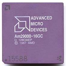
The first 29000 was released in 1988, including a built-in MMU but floating point support was offloaded to the 29027 FPU. Units with failed MMU's or BTC's were sold as the 29005.
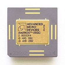
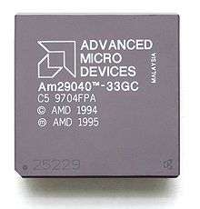
The line was upgraded with the 29030 and 29035, which included an 8 KB or 4 KB of instruction cache, respectively. Another update integrated the FPU on-die and added a 4 KB data cache to produce the 29040.
The last general-purpose version was the 29050. This was a significant upgrade to the original design, the first superscalar version which could execute instructions out-of-order and speculatively. Up to six instructions could be worked on at the same time through various pipeline stages, and four could be retired at any cycle. The 29050 also included a significantly improved FPU. The 29050 was initially available with clock rates of 25, 50, and 75 MHz. A 100 MHz version was introduced later.[1]
Several portions of the 29050 design were used as the basis for the K5 series of x86-compatible processors. The FPU adder and multiplier were carried over with some layout changes, a nanocode engine was added to the FPU to accommodate the complex instructions found in x86 but not on the 29050, while the rest of the core design was used along with complex microcode to translate x86 instructions to 29k-like 'uops' on the fly.
The Honeywell 29KII is a cpu based on the AMD 29050, and it was extensively used in real-time avionics.
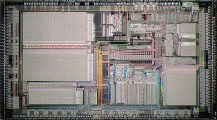
- Die photos
- Am29000
 Am29030
- Am29040
- Am29050
References
- Detar, Jim (31 October 1994). "AMD brews up Superscalar 29K". Electronic News.
External links
- AMD 29k (Streamlined Instruction Processor) ID Guide
- Mann, Daniel (1995), Evaluating and Programming the 29K RISC Family (PDF), Advanced Micro Devices, archived from the original (PDF) on September 27, 2007 pdf book about 29k family
- chipdb.org Images of different Am29000 processors