Athlon
Athlon is the brand name applied to a series of x86-compatible microprocessors designed and manufactured by Advanced Micro Devices (AMD). The original Athlon (now called Athlon Classic) was the first seventh-generation x86 processor and was the first desktop processor to reach speeds of one gigahertz (GHz). It made its debut as AMD’s high-end processor brand on June 23, 1999.[1] Over the years AMD has used the Athlon name with the 64-bit Athlon 64 architecture, the Athlon II, and Accelerated Processing Unit (APU) chips targeting the Socket AM1 desktop SoC architecture, and Socket AM4 Zen microarchitecture.[2] The modern Zen-based Athlon with a Radeon Graphics processor was introduced in 2019 as AMD’s highest-performance entry-level processor.[3][4]
AMD Athlon logo used for Zen-based models. | |
| General Info | |
|---|---|
| Launched | September 6, 2018 |
| Discontinued | |
| Common manufacturer(s) | |
| Performance | |
| Max. CPU clock rate | to 3.5 GHz |
| FSB speeds | to |
| Architecture and classification | |
| Min. feature size | 12 nm to |
| Instruction set | Zen (with Radeon Graphics) |
| Products, models, variants | |
| Core name(s) |
|
| History | |
| Predecessor | Athlon Classic Athlon Thunderbird Athlon XP/MP Athlon 64 Athlon 64 X2 Athlon X2 Athlon II |
Athlon comes from the Ancient Greek ἆθλον (athlon) meaning "(sport) contest", or "prize of a contest", or "place of a contest; arena".[5] With the Athlon name originally used for AMD's mid-range processors[2] with combined CPU/GPU processors with the GPU disabled,[6] AMD currently uses Athlon for budget APUs[2] with integrated graphics.[6] AMD positions the Athlon against its rival, the Intel Pentium.[7]
Brand history
K7 design and development
The first Athlon processor was a result of AMD's development of K7 processors in the 1990s. AMD founder and then-CEO Jerry Sanders[8] aggressively pursued strategic partnerships and engineering talent in the late 1990s, working to build on earlier successes in the PC market with the AMD K6 processor line.[9][10] One major partnership announced in 1998 paired AMD with semiconductor giant Motorola[8] to co-develop copper-based semiconductor technology, resulting in the K7 project being the first commercial processor to utilize copper fabrication technology. In the announcement, Sanders referred to the partnership as creating a "virtual gorilla" that would enable AMD to compete with Intel on fabrication capacity while limiting AMD's financial outlay for new facilities.[8] The K7 design team was led by Dirk Meyer, who had previously worked as a lead engineer at DEC on multiple Alpha microprocessors. When DEC was sold to Compaq in 1998 and discontinued Alpha processor development, and Sanders brought most of the Alpha design team to the K7 project. This added to the previously acquired NexGen K6 team, which already included engineers such as Vinod Dham.[11]
Original release
The AMD Athlon processor launched on June 23, 1999, with general availability by August 1999. Subsequently, from August 1999 until January 2002, this initial K7 processor was the fastest x86 chip in the world.[1] Wrote the Los Angeles Times on October 5, 1999, "AMD has historically trailed Intel’s fastest processors, but has overtaken the industry leader with the new Athlon. Analysts say the Athlon, which will be used by Compaq Computer, IBM and other manufacturers in their most powerful PCs, is significantly faster than Intel’s flagship Pentium III, which runs at a top speed of 600MHz."[12] A number of features helped the chips compete with Intel. By working with Motorola, AMD had been able to refine copper interconnect manufacturing about one year before Intel, with the revised process permitting 180-nanometer processor production. The accompanying die-shrink resulted in lower power consumption, permitting AMD to increase Athlon clock speeds to the 1 GHz range.[13] The Athlon architecture also used the EV6 bus licensed from DEC as its main system bus, allowing AMD to develop its own products without needing to license Intel's GTL+ bus.[14] By the summer of 2000, AMD was shipping Athlons at high volume and the chips were being used in systems by Gateway, Hewlett-Packard, and Fujitsu Siemens Computers among others.[15]
Later Athlon iterations
The second generation Athlon, the Thunderbird, debuted in 2000. AMD released the Athlon XP the following year,[1] and the Athlon XP's immediate successor, the Athlon 64, was an AMD64-architecture microprocessor released in 2003.[16] While the Athlon name was originally used for combined CPU/GPU processors with the GPU disabled,[6][2] after the 2007 launch of the Phenom processors, the Athlon name was also used for mid-range processors, positioned above brands such as Sempron.[17] The Athlon 64 X2 was released in 2005 as the first native dual-core desktop CPU designed by AMD,[18] and the Athlon X2 was a subsequent family based on the Athlon 64 X2.[19] Introduced in 2009, Athlon II was a dual-core family of Athlon chips.[20]
A USD$55 low-power Athlon 200GE with a Radeon graphics processor was introduced in September 2018, sitting under the Ryzen 3 2200G.[2] This iteration of Athlon used AMD’s Zen-based Raven Ridge core, which in turn had debuted in Ryzen with Radeon graphics processors.[6] With the release, AMD began using the Athlon brand name to refer to "low cost, high volume products," in a situation similar to both Intel's Celeron and Pentium Gold.[2] The modern Athlon 3000G was introduced in 2019, and was positioned as AMD’s highest-performance entry-level processor.[3] AMD positions the Athlon against it’s rival, the Intel Pentium. While CPU processing performance is in the same ballpark,[7] the Athlon 3000G uses Radeon Vega graphics,[3] which are rated as more powerful than the Pentium’s Intel UHD Graphics.[7]
Generations
Athlon Classic (1999)
The logo of the Athlon "Classic" | |
| General Info | |
|---|---|
| Launched | June 23, 1999 |
| Discontinued | |
| Common manufacturer(s) |
|
| Performance | |
| Max. CPU clock rate | 500 MHz to 2.33 GHz |
| FSB speeds | 200 MT/s to 400 MT/s |
| Architecture and classification | |
| Min. feature size | 0.25 μm to 0.13 μm |
| Instruction set | x86 |
| Physical specifications | |
| Socket(s) | |
| Products, models, variants | |
| Core name(s) |
|
| History | |
| Predecessor | K6-III |
| Successor | Athlon XP |
The AMD Athlon processor launched on June 23, 1999, with general availability by August 1999. Subsequently, from August 1999 until January 2002, this initial K7 processor was the fastest x86 chip in the world.[1] At launch it was, on average, 10% faster than the Pentium III at the same clock for business applications, and 20% faster for gaming workloads.[21] In commercial terms, the Athlon "Classic" was an enormous success.[22]
- Features

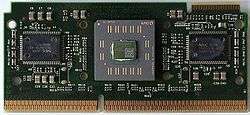
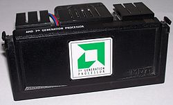
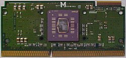
The Athlon Classic is a cartridge-based processor, named Slot A and similar to Intel's cartridge Slot 1 used for Pentium II and Pentium III. It used the same, commonly available, physical 242 pin connector used by Intel Slot 1 processors but rotated by 180 degrees to connect the processor to the motherboard. The cartridge assembly allowed the use of higher speed cache memory modules than could be put on (or reasonably bundled with) motherboards at the time. Similar to the Pentium II and the Katmai-based Pentium III, the Athlon Classic contained 512 KB of L2 cache. This high-speed SRAM cache was run at a divisor of the processor clock and was accessed via its own 64-bit back-side bus, allowing the processor to service both front-side bus requests and cache accesses simultaneously, as compared to pushing everything through the front-side bus.[23]
The Argon-based Athlon contained 22 million transistors and measured 184 mm2. It was fabricated by AMD in a version of their CS44E process, a 0.25 μm complementary metal–oxide–semiconductor (CMOS) process with six levels of aluminium interconnect.[24][25] "Pluto" and "Orion" Athlons were fabricated in a 0.18 μm process.[26]
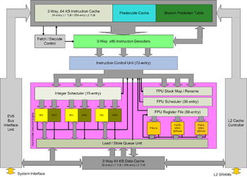
The Athlon's CPU cache consisted of the typical two levels. Athlon was the first x86 processor with a 128 KB[27] split level 1 cache; a 2-way associative cache separated into 2×64 KB for data and instructions (a concept from Harvard architecture).[28] SRAM cache designs at the time were incapable of keeping up with the Athlon's clock scalability, resulting in compromised CPU clock speeds in some computers.[29] With later Athlon models, AMD would integrate the L2 cache onto the processor itself, removing dependence on external cache chips.[26] The Slot-A Athlons were the first multiplier-locked CPUs from AMD, letting users set their own desired clock speed. This was done by AMD in part to hinder CPU remarking and overclocking by resellers, which could result in inconsistent performance. Eventually a product called the "Goldfingers device" was created that could unlock the CPU.[30]
AMD designed the CPU with more robust x86 instruction decoding capabilities than that of K6, to enhance its ability to keep more data in-flight at once.[28] The critical branch predictor unit was enhanced compared to the K6. Deeper pipelining with more stages allowed higher clock speeds to be attained.[31] Like the AMD K5 and K6, the Athlon dynamically buffered internal micro-instructions at runtime resulting from parallel x86 instruction decoding. The CPU is an out-of-order design, again like previous post-5x86 AMD CPUs. The Athlon utilizes the Alpha 21264's EV6 bus architecture with double data rate (DDR) technology.
AMD ended its long-time handicap with floating point x87 performance by designing a super-pipelined, out-of-order, triple-issue floating point unit (FPU).[28] Each of its three units could independently calculate an optimal type of instructions with some redundancy, making it possible to operate on more than one floating point instruction at once.[28] This FPU was a huge step forward for AMD, helping compete with Intel's P6 FPU.[32] The 3DNow! floating point SIMD technology, again present, received some revisions and was renamed "Enhanced 3DNow!" Additions included DSP instructions and the extended MMX subset of Intel SSE.[33]
- Specifications
- L1-cache: 64 + 64 KB (data + instructions)
- L2-cache: 512 KB, external chips on CPU module with 50%, 40% or 33% of CPU speed
- MMX, 3DNow!
- Slot A (EV6)
- Front-side bus: 200 MT/s (100 MHz double-pumped)
- VCore: 1.6 V (K7), 1.6–1.8 V (K75)
- First release: June 23, 1999 (K7), November 29, 1999 (K75)
- Clock-rate: 500–700 MHz (K7), 550–1000 MHz (K75)
Athlon Thunderbird (2000-2001)
The second generation Athlon, the Thunderbird or T-Bird, debuted on June 4, 2000.[1] This version of the Athlon had a traditional pin-grid array (PGA) format that plugged into a socket ("Socket A") on the motherboard or the slot A package. The major difference between it and the Athlon Classic was cache design, with AMD adding in 256 KB of on-chip, full-speed exclusive cache.[34] In moving to an exclusive cache design, the L1 cache's contents were not duplicated in the L2, increasing total cache size and functionally creating a large L1 cache with a slower region (the L2) and a fast region (the L1),[35] making the L2 cache into basically a victim cache. With the new cache design, need for high L2 performance and size was lessened, and the simpler L2 cache was less likely to cause clock scaling and yield issues. Thunderbird also moved to a 16-way associative layout.[34]
The Thunderbird was "cherished by many for its overclockability," and proved commercially successful,[11] as AMD's most successful product since the Am386DX-40 ten years earlier.[36] AMD's new fab facility in Dresden increased production for AMD overall and put out Thunderbirds at a fast rate, with the process technology improved by a switch to copper interconnects.[37] After several versions were released in 2000 and 2001 of the Thunderbird, the last Athlon processor using the Thunderbird core was released in 2001 in the summer, at which point speeds were at 1.4 Ghz.[1]
- Specifications
- L1-cache: 64 + 64 KB (data + instructions)
- L2-cache: 256 KB, full speed
- MMX, 3DNow!
- Slot A & Socket A (EV6)
- Front-side bus: 100 MHz (Slot-A, B-models), 133 MHz (C-models) (200 MT/s, 266 MT/s)
- VCore: 1.70–1.75 V
- First release: June 5, 2000
- Transistor count: 37 million
- Manufacturing Process: 0.18 μm/180 nm
- Clockrate:
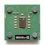
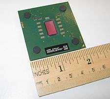
Athlon XP (2000-2003)
AMD Athlon logo used for Zen-based models. | |
| General Info | |
|---|---|
| Launched | October 9, 2001 |
| Products, models, variants | |
| Variant(s) | Palomino Thoroughbred Thorton Barton Corvette Dublin |
| History | |
| Predecessor | Athlon Thunderbird |
| Successor | Athlon 64 |
Overall, there are four main variants of the Athlon XP desktop CPU: the Palomino, the Thoroughbred, the Thorton, and the Barton. A number of mobile processors were also released, including the Corvette models, and the Dublin model among others.
Palomino

On May 14, 2001, AMD released the Athlon XP processor. It first debuted as the Mobile Athlon 4, a mobile version codenamed Corvette with the desktop Athlon XP released in the fall.[1] The third-generation Athlon, code-named Palomino, came out on October 9, 2001 as the Athlon XP, with the suffix signifying extended performance and unofficially referencing Windows XP.[38] Palomino's design used 180 nm fabrication process size.[26] The Athlon XP was marketed using a performance rating (PR) system comparing it to the Thunderbird predecessor core.[39] Among other changes, Palomino consumed 20% less power than the Thunderbird, comparatively reducing heat output,[40] and was roughly 10% faster than Thunderbird. Palomino also had enhanced K7's TLB architecture and included a hardware data prefetch mechanism to take better advantage of memory bandwidth. Palomino was the first K7 core to include the full SSE instruction set from the Intel Pentium III, as well as AMD's 3DNow! Professional.[41] Palomino was also the first socketed Athlon officially supporting dual processing, with chips certified for that purpose branded as the Athlon MP,[22] which had different specifications.[42] According to HardwareZone, it was possible to modify the Athlon XP to function as an MP.[43][44]
- Specifications
- L1-cache: 64 + 64 KB (data + instructions)
- L2-cache: 256 KB, full speed
- MMX, 3DNow!, SSE
- Socket A (EV6)
- Front-side bus: 133 MHz (266 MT/s)
- VCore: 1.50 to 1.75 V
- Power consumption: 68 W
- First release: October 9, 2001
- Clock-rate:
- Athlon 4: 850–1400 MHz
- Athlon XP: 1333–1733 MHz (1500+ to 2100+)
- Athlon MP: 1000–1733 MHz
Thoroughbred

The fourth-generation of Athlon was introduced with the Thoroughbred core, or T-Bred, on April 17, 2002.[45] The Thoroughbred core marked AMD's first production 130 nm silicon, with smaller die size than its predecessor.[26] There came to be two steppings (revisions) of this core commonly referred to as Tbred-A and Tbred-B.[45] Introduced in June 2002, the initial A version was mostly a direct die shrink of the preceding Palomino core, but did not significantly increase clock speeds over the Palomino.[26] A revised Thoroughbred core, Thoroughbred-B, added a ninth "metal layer" to the eight-layered Thoroughbred-A, offering improvement in headroom over the A and making it popular for overclocking.[46]
- Specifications
- L1-cache: 64 + 64 KB (data + instructions)
- L2-cache: 256 KB, full speed
- MMX, 3DNow!, SSE
- Socket A (EV6)
- Front-side bus: 133/166 MHz (266/333 MT/s)
- VCore: 1.50–1.65 V
- First release: June 10, 2002 (A), August 21, 2002 (B)
- Clock-rate:
- Thoroughbred "A": 1400–1800 MHz (1600+ to 2200+)
- Thoroughbred "B": 1400–2250 MHz (1600+ to 2800+)
- 133 MHz FSB: 1400–2133 MHz (1600+ to 2600+)
- 166 MHz FSB: 2083–2250 MHz (2600+ to 2800+)
Barton
Fifth-generation Athlon Barton-core processors were released in early 2003. While not operating at higher clock rates than Thoroughbred-core processors, they featured an increased L2 cache, and later models had an increased 200 MHz (400 MT/s) front side bus.[47] The Thorton core, a portmanteau of Thoroughbred and Barton, was a later variant of the Barton with half of the L2 cache disabled.[48] The Barton was used to officially introduce a higher 400 MT/s bus clock for the Socket A platform, which was used to gain some Barton models more efficiency.[47] By this point with the Barton, the four-year-old Athlon EV6 bus architecture had scaled to its limit and required a redesign to exceed the performance of newer Intel processors.[47] By 2003, the Pentium 4 had become more than competitive with AMD's processors,[49] and Barton only saw a small performance increase over the Thoroughbred-B it derived from,[47] insufficient to outperform the Pentium 4.[49] The K7 derived Athlons such as Barton were replaced in September 2003 by the Athlon 64 family, which featured an on-chip memory controller and a new HyperTransport bus.[50]
- Specifications
Barton (130 nm)
- L1-cache: 64 + 64 KB (data + instructions)
- L2-cache: 512 KB, full speed
- MMX, 3DNow!, SSE
- Socket A (EV6)
- Front-side bus: 166/200 MHz (333/400 MT/s)
- VCore: 1.65 V
- First release: February 10, 2003
- Clockrate: 1833–2333 MHz (2500+ to 3200+)
- 166 MHz FSB: 1833–2333 MHz (2500+ to 3200+)
- 200 MHz FSB: 2100, 2200 MHz (3000+, 3200+)
Thorton (130 nm)
- L1-cache: 64 + 64 KB (Data + Instructions)
- L2-cache: 256 KB, full speed
- MMX, 3DNow!, SSE
- Socket A (EV6)
- Front-side bus: 133/166/200 MHz (266/333/400 MT/s)
- VCore: 1.50–1.65 V
- First release: September 2003
- Clockrate: 1667–2200 MHz (2000+ to 3100+)
- 133 MHz FSB: 1600–2133 MHz (2000+ to 2600+)
- 166 MHz FSB: 2083 MHz (2600+)
- 200 MHz FSB: 2200 MHz (3100+)
Mobile Athlon XP
The Palomino core debuted in the mobile market before the PC market, where it was branded as Mobile Athlon 4 with the codename "Corvette". It distinctively used a ceramic interposer much like the Thunderbird instead of the organic pin grid array package used on all later Palomino processors.[41] In November 2001, AMD released a 1.2GHz Athlon 4 and a 950MHz Duron.[51] The Mobile Athlon 4 processors included the PowerNow! function, which controlled a laptop's "level of processor performance by dynamically adjusting its operating frequency and voltage according to the task at hand,"[52] thus extending "battery life by reducing processor power when it isn't needed by applications." Duron chips also included PowerNow![51] In 2002, AMD released a version of PowerNow! called Cool'n'Quiet, implemented on the Athlon XP but only adjusting clock speed frequency instead of voltage.[53]
In 2002 the Athlon XP-M (Mobile Athlon XP) replaced the Mobile Athlon 4 using the newer Thoroughbred core,[54] with Barton cores for full-size notebooks. The Athlon XP-M was also offered in a compact microPGA socket 563 version.[55] Mobile XPs were not multiplier-locked, making them popular with desktop overclockers.[56]
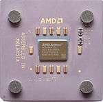
Athlon 64 (2003-2009)
The immediate successor to the Athlon XP, the Athlon 64 is an AMD64-architecture microprocessor produced by AMD, released on September 23, 2003.[16] A number of variations, all named after cities, were released with 90 nm architecture in 2004 and 2005. Versions released in 2007 and 2009 utilized 65 nm architecture.
Athlon 64 X2 (2005-2009)
The Athlon 64 X2 was released in 2005 as the first native dual-core desktop CPU designed by AMD using an Athlon 64.[18] The Athlon X2 was a subsequent family of microprocessors based on the Athlon 64 X2. The original Brisbane Athlon X2 models used 65 nm architecture, and were released in 2007.[19]
Athlon II (2009-2012)
Athlon II is a family of central processing units. Initially a dual-core version of the Athlon II, the K-10-based Regor was released in June 2009 with 45 nanometer architecture. This was followed by a single-core version, Sargas,[20] followed by the quad-core Propus, the triple-core Rana in November 2009,[57] and the Llano 32 nm version released in 2011.[58]
Zen-based Athlon (2018-present)
The Zen-based Athlon with Radeon graphics processors was launched in September 2018 with the Athlon 200GE.[59] Based on AMD’s Raven Ridge core previously used in variants of the Ryzen 3 and Ryzen 5,[6] the Athlon 200GE had half of the cores but left SMT enabled. It also kept the same 4 mb L3 cache,[59] but the L1 cache was halved to 1 mb.[60]
In addition, the number of graphics compute units was limited to 3 in the Athlon 200GE,[61] and the chip was multiplier-locked.[62] Despite its limitations, the Athlon 200GE performed competitively against[63] the 5000-series Intel Pentium-G, displaying similar CPU performance but an advantage in GPU performance.[64]
On November 19, 2019, AMD released the Athlon 3000G, with a higher 3.5 GHz core clock and 1100MHz graphics clock compared to the Athlon 200GE[3] also with two cores.[4] The main functional difference between the 200GE was the Athlon 3000G’s unlocked multiplier,[3] allowing the latter to be overclocked on B450 and X470 motherboards.[65]
Specifications (see Zen desktop APUs for more details)[60]
Raven Ridge (14 nm), Picasso (12nm)
- L1 Cache: 192kb (2x64KiB +2x32KiB)
- L2-cache: 1MB (2x512KiB)
- L3 Cache: 4MB
- Memory: Dual-Channel DDR4-2666, 64GB Max
- Socket AM4
- TDP: 35W
- First release: September 6, 2018
- CPU Clockrate: 3.2 to 3.5 GHz
- GPU Clockrate: 1000 to 1100 MHz
Supercomputers
A number of supercomputers have been built using Athlon chips, largely at universities. Among them:
- In 2000, several American students claimed to have built the world's least expensive supercomputer by clustering 64 AMD Athlon chips together, also marking the first time Athlons had been clustered in a supercomputer.[66]
- The PRESTO III, a Beowulf cluster of 78 AMD Athlon processors, was built by in 2001 the Tokyo Institute of Technology. That year it ranked 439 on the Top 500 list of supercomputers.[67]
- In 2002, a "128-Node 256-Processor AMD Athlon Supercomputer Cluster" was installed at the Ohio Supercomputer Center at the University of Toledo.[68]
- Rutgers University, Department of Physics & Astronomy. Machine: NOW Cluster—AMD Athlon. CPU: 512 AthlonMP (1.65 GHz). Rmax: 794 GFLOPS.
See also
References
This article is based on material taken from the Free On-line Dictionary of Computing prior to 1 November 2008 and incorporated under the "relicensing" terms of the GFDL, version 1.3 or later.
- "cpu-collection.de >> AMD >> athlon". www.cpu-collection.de. Retrieved February 24, 2017.
- "AMD Announces New $55 Low-Power Processor: Athlon 200GE". AnandTech. Retrieved September 6, 2018.
- Lucian Armasu (November 19, 2019). "AMD's Unlocked Athlon 3000G APU Starts Shipping at $49". Tom's Hardware.
- Hilbert Hagedoorn (December 3, 2019). "AMD Athlon 3000G review". Guru3D.
- ἆθλον. Liddell, Henry George; Scott, Robert; A Greek–English Lexicon at the Perseus Project.
- "Two New 35W Raven Ridge Parts: AMD Athlon 200GE and Athlon Pro 200GE". Anandtech. May 26, 2018. Retrieved August 4, 2020.
- Kevin Carbotte (March 4, 2019). "AMD Athlon vs Intel Pentium: Which Cheap Chips Are Best?". Tom's Hardware. Retrieved August 4, 2020.
- "Motorola Prepares to Manufacture AMD's Upcoming K7 Chip". HP. August 7, 1998. Archived from the original on September 28, 2007.
- CNET News Staff (April 7, 1998). "IBM PCs tout AMD chips". CNET. Retrieved August 4, 2020.
- "The Next Big Thing". The Wall Street Journal. August 5, 2002. Retrieved August 4, 2020.
- Graham Singer (November 21, 2012). "The Rise and Fall of AMD". TechSpot. Retrieved August 3, 2020.
- Charles Piller (October 5, 1999). "AMD Boosts Lead Over Intel With New Version of Its Athlon Chip". Los Angeles Times. Retrieved August 4, 2020.
- AMD Announces First Revenue Shipments From Dresden "MEGAFAB", AMD Press Release, June 5, 2000, retrieved January 6, 2012
- Gary Mauler, Milt Beebe (December 19, 2001). "I/O subsystems and capacity planning for clusters". Clustering Windows Server: A Road Map for Enterprise Solutions. Retrieved August 4, 2020.
- Richard Ricthmyer (August 28, 2000). "AMD's chips hit high gear". CNN. Retrieved August 4, 2020.
- John G. Spooner (September 23, 2003). "AMD's Athlon steps up to 64 bits". Cnet. Retrieved August 3, 2020.
- "AMD Athlon/Duron/Sempron CPU identification and OPN breakdown", amdboard.com
- Tony Smith (May 31, 2005). "AMD launches dual-core Athlon 64 X2". The Register. Retrieved August 3, 2020.
- Jeff Bouton (June 5, 2007). "AMD Athlon X2 BE-2350 and BE-2300 "Brisbane" Processors". Hot Hardware. Retrieved August 3, 2020.
- "AMD Regor Core". CPU World. 2009. Retrieved August 3, 2020.
- Lal Shimpi, Anand (August 9, 1999), AMD Athlon, retrieved January 6, 2012,
The performance of the K7, then clocked at 500MHz, was on par with a Pentium III 500.
- Lal Shimpi, Anand (June 5, 2001), AMD 760MP & Athlon MP – Dual Processor Heaven, Anandtech, retrieved January 6, 2012
- De Gelas, Johan (September 29, 1999), Clash of Silicon, The Athlon 650, Ace's Hardware, archived from the original on December 25, 2001, retrieved January 6, 2012
- Golden, Michael; et al. (1999), "A Seventh-Generation x86 Microprocessor", IEEE Journal of Solid-State Circuits, 34 (11): 1466–1477, doi:10.1109/4.799851
- Keith Diefendorff (October 26, 1998), "K7 Challenges Intel" (PDF), Microprocessor Report, 12 (14), retrieved January 6, 2012
- Robert Bruce Thompson, Barbara Fritchman (July 24, 2003). "PC Hardware in a Nutshell: A Desktop Quick Reference". Thompson. Retrieved August 4, 2020.
- Transistorized memory, such as RAM, ROM, flash and cache sizes as well as file sizes are specified using binary meanings for K (10241), M (10242), G (10243), ...
- Paul Hsieh (August 11, 1999), 7th Generation CPU Comparisons, retrieved January 6, 2012
- Lal Shimpi, Anand (March 6, 2000), AMD Athlon 1 GHz, 950 MHz, 900 MHz, Anandtech, p. 2
- Jim Noonan; James Rolfe (March 21, 2000), Athlon Gold-Finger Devices, Overclockers.com.au, archived from the original on February 1, 2009, retrieved January 6, 2012
- De Gelas, Johan. The Secrets of High Performance CPUs, Part 1, Ace's Hardware, September 29, 1999.
- Pabst, Thomas (August 23, 1999), Performance-Showdown between Athlon and Pentium III, Tom's Hardware, retrieved January 6, 2012
- Womack, Tom, Extensions to the x86 architecture, archived from the original on January 15, 2012, retrieved January 6, 2012
- K7 microarchitecture information, Sandpile.org, archived from the original on October 13, 1999, retrieved January 6, 2012
- Stokes, John (February 1, 2005), Inside AMD's Hammer: the 64-bit architecture behind the Opteron and Athlon 64, Ars Technica, p. 9, retrieved January 6, 2012
- "The Red Hill CPU Guide: transition to the 386". www.redhill.net.au. Retrieved June 6, 2020.
- Jack Robertson (April 24, 2000). "Dresden fab is putting AMD back on the manufacturing map". EE Times. Retrieved August 4, 2020.
- Introducing the AMD Athlon XP Processor (PDF), Advanced Micro Devices, Inc., archived from the original (PDF) on September 27, 2007, retrieved January 6, 2012
- Wasson, Scott (November 5, 2001), AMD's Athlon XP 1900+ processor: Pouring it on, The Tech Report, p. 1, retrieved January 6, 2012
- Wasson, Scott (October 9, 2001), AMD's Athlon XP 1800+ processor: 1533 > 1800, The Tech Report, retrieved January 6, 2012
- Lal Shimpi, Anand (May 14, 2001), AMD Athlon 4 – The Palomino is Here, Anandtech, pp. 4–5, retrieved January 6, 2012
- "AMD's Technical Specifications] for 7th generation CPUs" (PDF). AMD. 2003.
- Jimmy Tang (March 15, 2002). "Modding the Athlon XP into an MP". Hardware Zone.
- Jimmy Tang (May 12, 2003). "Modding the Barton XP to a Barton MP". Hardware Zone.
- AMD Athlon Thoroughbred core, May 2, 2011, retrieved January 6, 2012
- Lal Shimpi, Anand (August 21, 2002), Introducing Thoroughbred Revision B, Anandtech, retrieved January 6, 2012
- De Gelas, Johan (February 10, 2003), Barton: 512 KB Athlon XP Reviewed, Ace's Hardware, archived from the original on March 24, 2003, retrieved January 6, 2012
- http://www.cpu-world.com/Cores/Thorton.html
- Lal Shimpi, Anand (February 10, 2003), AMD's Athlon XP 3000+: Barton cuts it close, AnandTech, retrieved January 6, 2012
- Scott Wasson (January 6, 2020). "AMD's Athlon 64 3400+ process". The Tech Report. Retrieved August 4, 2020.
- Matthew Broersma (November 13, 2001). "XP blacks out AMD power management". ZDNet. Retrieved August 3, 2020.
- Steven Parker (October 19, 2001). "Windows XP Patch: AMD Power Now availability in XP". Neowin. Retrieved August 3, 2020.
- Mark Hachmann (January 25, 2002). "AMD Offering Version of PowerNow! For Athlon XP". ExtremeTech. Retrieved August 3, 2020.
- March Hachmann (April 17, 2002). "Update: AMD Launches Mobile Athlon XP". Extreme Tech. Retrieved August 3, 2020.
- Mark Hachman (March 12, 2003). "Update AMD Announces Mobile Athlon XP". Extreme Tech. Retrieved August 3, 2020.
- Don Woligroski (2013). "14 Of The Most Legendary Overclocking-Friendly CPUs". Tom's Hardware. Retrieved August 3, 2020.
- Patrick Schmid and Achim Roos (September 16, 2009). "AMD Athlon II X4 620: Quad Core For The Masses At $100". Tom's Hardware. Retrieved August 3, 2020.
- Don Woligroski (January 30, 2012). "Picking A Sub-$200 Gaming CPU: FX, An APU, Or A Pentium?". Tom's Hardware. Retrieved August 3, 2020.
- Anton Shilov (September 21, 2018). "AMD's Athlon 22GE Processors Now Available". Anandtech. Retrieved August 3, 2020.
- "AMD Athlon 200GE / 3.2 GHz processor Specs & Prices". CNET. Retrieved August 3, 2020.
- "AMD Reimagines Everyday Computing with New "Zen" Based Athlon™ Desktop Processors, Expands Commercial Client Portfolio with 2nd Generation Ryzen™ PRO Desktop Processors". AMD. September 6, 2018. Retrieved August 4, 2020.
- Hilbert Hagedoorn (December 21, 2018). "AMD Athlon 200GE review". Guru3D. Retrieved August 4, 2020.
- "The Best Entry Level Gaming CPU: Athlon 200GE vs. Pentium G5400 vs. Ryzen 3 2200G". Tech Spot. November 2, 2018. Retrieved August 4, 2020.
- Kevin Carbotte (December 19, 2018). "AMD Athlon 200GE vs. Intel Pentium Gold G5400: Cheap CPU Showdown". Tom's Hardware. Retrieved August 4, 2020.
- Joel Hruska (November 20, 2019). "AMD Launches Budget Athlon 3000G With $49 Overclocking Support". Extreme Tech.
- "Students build super cheap supercomputer". Computing. June 8, 2000. Retrieved August 2, 2020.
- Drew Cullen (July 2, 2001). "AMD cluster sneaks in Supercomputer top 500 list". The Register. Retrieved August 2, 2020.
- "Ohio Supercomputer Center Awards Cluster to University of Toledo". Ohio Supercomputer Center. August 6, 2004. Retrieved August 2, 2020.