AMD K6-2
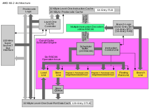
The K6-2 is an x86 microprocessor introduced by AMD on May 28, 1998,[2] and available in speeds ranging from 266 to 550 MHz. An enhancement of the original K6, the K6-2 introduced AMD's 3DNow! SIMD instruction set, featured a larger 64 KiB Level 1 cache (32 KiB instruction and 32 KiB data), and an upgraded system-bus interface called Super Socket 7, which was backward compatible with older Socket 7 motherboards. It was manufactured using a 0.25 micrometre process, ran at 2.2 volts, and had 9.3 million transistors.
 | |
| General Info | |
|---|---|
| Launched | May 28, 1998 |
| Discontinued | end of 2003 [1] |
| Common manufacturer(s) | |
| Performance | |
| Max. CPU clock rate | 200 MHz to 550 MHz |
| FSB speeds | 66 MHz to 100 MHz |
| Architecture and classification | |
| Min. feature size | 0.25 μm |
| Microarchitecture | x86 |
| Instruction set | MMX, 3DNow! |
| Physical specifications | |
| Cores |
|
| Socket(s) | |
| Products, models, variants | |
| Core name(s) |
|
| History | |
| Predecessor | K6 |
| Successor | K6-III |
.jpg)
History

The K6-2 was designed as a competitor to Intel's flagship processor, the significantly more expensive Pentium II. Performance of the two chips was similar: the previous K6 tended to be faster for general-purpose computing, while the Intel part was faster in x87 floating-point applications. To battle the Pentium 2's dominance on floating point calculations the K6-2 was the first CPU to introduce a floating point SIMD instruction set (dubbed 3DNow! by AMD), which significantly boosted performance. However programs needed to be specifically tailored for the new instructions and despite beating Intel's SSE instruction set to market, 3DNow achieved only limited popularity.
Super Socket 7, which increased the processor bus from 66 MHz to 100 MHz, allowed the K6-2 to withstand the effects of ever-increasing CPU multipliers fairly gracefully and in later life it remained surprisingly competitive. Nearly all K6-2s were designed to use 100 MHz Super Socket 7 mainboards, allowing the system-bus to keep pace with the K6-2's clock-frequency.
The K6-2 was a very financially successful chip and enabled AMD to earn the revenue it would need to introduce the forthcoming Athlon. The introductory K6-2 300 was by far the best-selling variant. It rapidly established an excellent reputation in the marketplace and offered a favorable price/performance ratio versus Intel's Celeron 300A. While the K6-2 had mediocre floating-point performance compared to the Celeron, it offered faster system RAM access (courtesy of the Super 7 mainboard), as well as 3DNow graphics extensions.
As the market moved on, AMD released a long series of faster K6-2 parts, the best-selling ones being the 350, 400, 450, and 500. By the time the 450 and the 500 were mainstream parts, the K6-2 family had already moved to the budget PC segment, where it still competed successfully against Intel's Celeron.
K6-2+
Despite the name, the little-known K6-2+ was based on the AMD K6-III+ design (model 13) with 128 KiB of integrated L2 cache and built on a 0.18 micrometre process (essentially a K6-III+ with half the L2 cache). The K6-2+ was specifically designed as a low-power mobile CPU. Some motherboard companies such as Gigabyte and FIC provided BIOS updates for their desktop motherboards to allow for usage of these processors; for other officially not supported mainboards, the community created unofficial BIOS updates on their own.[3][4]
Most K6-2+ motherboards did not support a clock multiplier setting greater than 5.5 since 550 MHz was the highest official speed of the K6-2+ (100*5.5 = 550) but a little known feature of the both the K6-2 and K6-2+ was that it interpreted the motherboard clock multiplier setting 2 as 6. This allowed many users to run their K6-2+ 550 MHz and often even a K6-2+ 500 MHz at a speed of 600 MHz simply by setting the motherboard clock multiplier to 2.[5]
Features
CPU features table
Models
K6-2 (Chomper, 250 nm)


- Package number: 26050
- CPUID: Family 5, Model 8, Stepping 0
- L1-Cache: 32 + 32 KiB (Data + Instructions)
- MMX, 3DNow!
- 9.3 million transistors
- Super Socket 7
- Front side bus: 66, 100 MHz
- VCore: 2.2V
- First release: May 28, 1998
- Manufacturing process: 0.25 μm
- Clockrate: 233, 266, 300, 333, 350 & 366 MHz
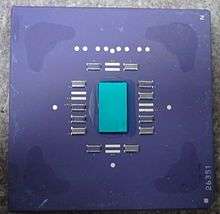
K6-2 (Chomper Extended (CXT), 250 nm)
- Package number: 26351
- CPUID: Family 5, Model 8, Stepping 12
- L1-Cache: 32 + 32 KiB (Data + Instructions)
- MMX, 3DNow!
- Super Socket 7
- Front side bus: 66, 95, 97, 100 MHz
- VCore: 2.0(mobile)/2.2/2.3/2.4V
- First release: November 16, 1998
- Manufacturing process: 0.25 μm
- Clockrate: 200, 233, 266, 300, 333, 350, 366, 380, 400, 427.5, 450, 475, 500, 533 & 550 MHz
References
- AMD to kill K6, K6-II, K6-III
- "AMD Introduces AMD-K6-2 Processor with New 3DNow! Technology". Advanced Micro Devices. 1998-05-28. Archived from the original on 2014-02-02.
- Soucek, Petr (2002-07-07). "Award BIOS Modifications". Retrieved 2017-07-19.
- Steunebrink, Jan (2008-07-02). "The Unofficial AMD K6-2+ / K6-III+ Page". Retrieved 2017-07-19.
- Völkel, Frank (2000-07-13). "600 MHz with Socket 7: The AMD K6-2+". Tom's Hardware. Retrieved 2017-07-19.
Further reading
- Khanna, R. et al. (1998). "A 0.25µm x86 microprocessor with a 100MHz Socket 7 interface". ISSCC Digest of Technical Papers, pp. 242–243.
External links
| Wikimedia Commons has media related to AMD K6-2. |