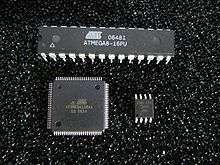
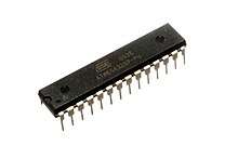
AVR microcontrollers
AVR is a family of microcontrollers developed since 1996 by Atmel, acquired by Microchip Technology in 2016. These are modified Harvard architecture 8-bit RISC single-chip microcontrollers. AVR was one of the first microcontroller families to use on-chip flash memory for program storage, as opposed to one-time programmable ROM, EPROM, or EEPROM used by other microcontrollers at the time.

AVR microcontrollers find many applications as embedded systems. They are especially common in hobbyist and educational embedded applications, popularized by their inclusion in many of the Arduino line of open hardware development boards.
History
The AVR architecture was conceived by two students at the Norwegian Institute of Technology (NTH),[1] Alf-Egil Bogen[2] and Vegard Wollan.[3]
Atmel says that the name AVR is not an acronym and does not stand for anything in particular. The creators of the AVR give no definitive answer as to what the term "AVR" stands for.[3] However, it is commonly accepted that AVR stands for Alf and Vegard's RISC processor.[4] Note that the use of "AVR" in this article generally refers to the 8-bit RISC line of Atmel AVR Microcontrollers.
The original AVR MCU was developed at a local ASIC house in Trondheim, Norway, called Nordic VLSI at the time, now Nordic Semiconductor, where Bogen and Wollan were working as students. It was known as a μRISC (Micro RISC)[5] and was available as silicon IP/building block from Nordic VLSI.[6] When the technology was sold to Atmel from Nordic VLSI, the internal architecture was further developed by Bogen and Wollan at Atmel Norway, a subsidiary of Atmel. The designers worked closely with compiler writers at IAR Systems to ensure that the AVR instruction set provided efficient compilation of high-level languages.[7]
Among the first of the AVR line was the AT90S8515, which in a 40-pin DIP package has the same pinout as an 8051 microcontroller, including the external multiplexed address and data bus. The polarity of the RESET line was opposite (8051's having an active-high RESET, while the AVR has an active-low RESET), but other than that the pinout was identical.
The AVR 8-bit microcontroller architecture was introduced in 1997. By 2003, Atmel had shipped 500 million AVR flash microcontrollers.[8] The Arduino platform, developed for simple electronics projects, was released in 2005 and featured ATmega8 AVR microcontrollers.
Device overview
The AVR is a modified Harvard architecture machine, where program and data are stored in separate physical memory systems that appear in different address spaces, but having the ability to read data items from program memory using special instructions.
Basic families
AVRs are generally classified into following:
- tinyAVR – the ATtiny series
- 0.5–32 KB program memory
- 6–32-pin package
- Limited peripheral set
- megaAVR – the ATmega series
- 4–256 KB program memory
- 28–100-pin package
- Extended instruction set (multiply instructions and instructions for handling larger program memories)
- Extensive peripheral set
- XMEGA – the ATxmega series
- 16–384 KB program memory
- 44–64–100-pin package (A4, A3, A1)
- 32-pin package: XMEGA-E (XMEGA8E5)
- Extended performance features, such as DMA, "Event System", and cryptography support
- Extensive peripheral set with ADCs
- Application-specific AVR
- megaAVRs with special features not found on the other members of the AVR family, such as LCD controller, USB controller, advanced PWM, CAN, etc.
- FPSLIC (AVR with FPGA)
- 32-bit AVRs
- In 2006, Atmel released microcontrollers based on the 32-bit AVR32 architecture. This was a completely different architecture unrelated to the 8-bit AVR, intended to compete with the ARM-based processors. It had a 32-bit data path, SIMD and DSP instructions, along with other audio- and video-processing features. The instruction set was similar to other RISC cores, but it was not compatible with the original AVR (nor any of the various ARM cores). Since then support for AVR32 has been dropped from Linux as of kernel 4.12; compiler support for the architecture in GCC was never mainlined into the compiler's central source code repository and was available primarily in a vendor-supported fork. At the time that AVR32 was introduced, Atmel had already been a licensee of the ARM architecture, with both ARM7 and ARM9 microcontrollers having been released prior to and concurrently with the AVR32; later Atmel focused most development effort on 32-bit chips with ARM Cortex-M and Cortex-A cores.
Device architecture
Flash, EEPROM, and SRAM are all integrated onto a single chip, removing the need for external memory in most applications. Some devices have a parallel external bus option to allow adding additional data memory or memory-mapped devices. Almost all devices (except the smallest TinyAVR chips) have serial interfaces, which can be used to connect larger serial EEPROMs or flash chips.
Program memory
Program instructions are stored in non-volatile flash memory. Although the MCUs are 8-bit, each instruction takes one or two 16-bit words.
The size of the program memory is usually indicated in the naming of the device itself (e.g., the ATmega64x line has 64 KB of flash, while the ATmega32x line has 32 KB).
There is no provision for off-chip program memory; all code executed by the AVR core must reside in the on-chip flash. However, this limitation does not apply to the AT94 FPSLIC AVR/FPGA chips.
Internal data memory
The data address space consists of the register file, I/O registers, and SRAM. Some small models also map the program ROM into the data address space, but larger models do not.
Internal registers
The AVRs have 32 single-byte registers and are classified as 8-bit RISC devices.
In the tinyAVR and megaAVR variants of the AVR architecture, the working registers are mapped in as the first 32 memory addresses (000016–001F16), followed by 64 I/O registers (002016–005F16). In devices with many peripherals, these registers are followed by 160 “extended I/O” registers, only accessible as memory-mapped I/O (006016–00FF16).
Actual SRAM starts after these register sections, at address 006016 or, in devices with "extended I/O", at 010016.
Even though there are separate addressing schemes and optimized opcodes for accessing the register file and the first 64 I/O registers, all can also be addressed and manipulated as if they were in SRAM.
The very smallest of the tinyAVR variants use a reduced architecture with only 16 registers (r0 through r15 are omitted) which are not addressable as memory locations. I/O memory begins at address 000016, followed by SRAM. In addition, these devices have slight deviations from the standard AVR instruction set. Most notably, the direct load/store instructions (LDS/STS) have been reduced from 2 words (32 bits) to 1 word (16 bits), limiting the total direct addressable memory (the sum of both I/O and SRAM) to 128 bytes. Conversely, the indirect load instruction's (LD) 16-bit address space is expanded to also include non-volatile memory such as Flash and configuration bits; therefore, the Load Program Memory (LPM) instruction is unnecessary and omitted. (For detailed info, see Atmel AVR instruction set.)
In the XMEGA variant, the working register file is not mapped into the data address space; as such, it is not possible to treat any of the XMEGA's working registers as though they were SRAM. Instead, the I/O registers are mapped into the data address space starting at the very beginning of the address space. Additionally, the amount of data address space dedicated to I/O registers has grown substantially to 4096 bytes (000016–0FFF16). As with previous generations, however, the fast I/O manipulation instructions can only reach the first 64 I/O register locations (the first 32 locations for bitwise instructions). Following the I/O registers, the XMEGA series sets aside a 4096 byte range of the data address space, which can be used optionally for mapping the internal EEPROM to the data address space (100016–1FFF16). The actual SRAM is located after these ranges, starting at 200016.
GPIO ports
Each GPIO port on a tiny or mega AVR drives up to eight pins and is controlled by three 8-bit registers: DDRx, PORTx and PINx, where x is the port identifier.
- DDRx: Data Direction Register, configures the pins as either inputs or outputs.
- PORTx: Output port register. Sets the output value on pins configured as outputs. Enables or disables the pull-up resistor on pins configured as inputs.
- PINx: Input register, used to read an input signal. On some devices, this register can be used for pin toggling: writing a logic one to a PINx bit toggles the corresponding bit in PORTx, irrespective of the setting of the DDRx bit.[10]
Newer ATtiny AVR's, like ATtiny817 and its siblings, have their port control registers somewhat differently defined. xmegaAVR have additional registers for push/pull, totem-pole and pullup configurations.
EEPROM
Almost all AVR microcontrollers have internal EEPROM for semi-permanent data storage. Like flash memory, EEPROM can maintain its contents when electrical power is removed.
In most variants of the AVR architecture, this internal EEPROM memory is not mapped into the MCU's addressable memory space. It can only be accessed the same way an external peripheral device is, using special pointer registers and read/write instructions, which makes EEPROM access much slower than other internal RAM.
However, some devices in the SecureAVR (AT90SC) family[11] use a special EEPROM mapping to the data or program memory, depending on the configuration. The XMEGA family also allows the EEPROM to be mapped into the data address space.
Since the number of writes to EEPROM is limited – Atmel specifies 100,000 write cycles in their datasheets – a well designed EEPROM write routine should compare the contents of an EEPROM address with desired contents and only perform an actual write if the contents need to be changed.
Note that erase and write can be performed separately in many cases, byte-by-byte, which may also help prolong life when bits only need to be set to all 1s (erase) or selectively cleared to 0s (write).
Program execution
Atmel's AVRs have a two-stage, single-level pipeline design. This means the next machine instruction is fetched as the current one is executing. Most instructions take just one or two clock cycles, making AVRs relatively fast among eight-bit microcontrollers.
The AVR processors were designed with the efficient execution of compiled C code in mind and have several built-in pointers for the task.
Instruction set
The AVR instruction set is more orthogonal than those of most eight-bit microcontrollers, in particular the 8051 clones and PIC microcontrollers with which AVR competes today. However, it is not completely regular:
- Pointer registers X, Y, and Z have addressing capabilities that are different from each other.
- Register locations R0 to R15 have more limited addressing capabilities than register locations R16 to R31.
- I/O ports 0 to 31 can be bit addressed, unlike I/O ports 32 to 63.
- CLR (clear all bits to zero) affects flags, while SER (set all bits to one) does not, even though they are complementary instructions. (CLR is pseudo-op for EOR R, R; while SER is short for LDI R,$FF. Arithmetic operations such as EOR modify flags, while moves/loads/stores/branches such as LDI do not.)
- Accessing read-only data stored in the program memory (flash) requires special LPM instructions; the flash bus is otherwise reserved for instruction memory.
Additionally, some chip-specific differences affect code generation. Code pointers (including return addresses on the stack) are two bytes long on chips with up to 128 KB of flash memory, but three bytes long on larger chips; not all chips have hardware multipliers; chips with over 8 KB of flash have branch and call instructions with longer ranges; and so forth.
The mostly regular instruction set makes programming it using C (or even Ada) compilers fairly straightforward. GCC has included AVR support for quite some time, and that support is widely used. In fact, Atmel solicited input from major developers of compilers for small microcontrollers, to determine the instruction set features that were most useful in a compiler for high-level languages.[7]
MCU speed
The AVR line can normally support clock speeds from 0 to 20 MHz, with some devices reaching 32 MHz. Lower-powered operation usually requires a reduced clock speed. All recent (Tiny, Mega, and Xmega, but not 90S) AVRs feature an on-chip oscillator, removing the need for external clocks or resonator circuitry. Some AVRs also have a system clock prescaler that can divide down the system clock by up to 1024. This prescaler can be reconfigured by software during run-time, allowing the clock speed to be optimized.
Since all operations (excluding multiplication and 16-bit add/subtract) on registers R0–R31 are single-cycle, the AVR can achieve up to 1 MIPS per MHz, i.e. an 8 MHz processor can achieve up to 8 MIPS. Loads and stores to/from memory take two cycles, branching takes two cycles. Branches in the latest "3-byte PC" parts such as ATmega2560 are one cycle slower than on previous devices.
Development
AVRs have a large following due to the free and inexpensive development tools available, including reasonably priced development boards and free development software. The AVRs are sold under various names that share the same basic core, but with different peripheral and memory combinations. Compatibility between chips in each family is fairly good, although I/O controller features may vary.
See external links for sites relating to AVR development.
Features
AVRs offer a wide range of features:
- Multifunction, bi-directional general-purpose I/O ports with configurable, built-in pull-up resistors
- Multiple internal oscillators, including RC oscillator without external parts
- Internal, self-programmable instruction flash memory up to 256 KB (384 KB on XMega)
- In-system programmable using serial/parallel low-voltage proprietary interfaces or JTAG
- Optional boot code section with independent lock bits for protection
- On-chip debugging (OCD) support through JTAG or debugWIRE on most devices
- The JTAG signals (TMS, TDI, TDO, and TCK) are multiplexed on GPIOs. These pins can be configured to function as JTAG or GPIO depending on the setting of a fuse bit, which can be programmed via ISP or HVSP. By default, AVRs with JTAG come with the JTAG interface enabled.
- debugWIRE uses the /RESET pin as a bi-directional communication channel to access on-chip debug circuitry. It is present on devices with lower pin counts, as it only requires one pin.
- Internal data EEPROM up to 4 KB
- Internal SRAM up to 16 KB (32 KB on XMega)
- External 64 KB little endian data space on certain models, including the Mega8515 and Mega162.
- The external data space is overlaid with the internal data space, such that the full 64 KB address space does not appear on the external bus and accesses to e.g. address 010016 will access internal RAM, not the external bus.
- In certain members of the XMega series, the external data space has been enhanced to support both SRAM and SDRAM. As well, the data addressing modes have been expanded to allow up to 16 MB of data memory to be directly addressed.
- 8-bit and 16-bit timers
- PWM output (some devices have an enhanced PWM peripheral which includes a dead-time generator)
- Input capture that record a time stamp triggered by a signal edge
- Analog comparator
- 10 or 12-bit A/D converters, with multiplex of up to 16 channels
- 12-bit D/A converters
- A variety of serial interfaces, including
- I²C compatible Two-Wire Interface (TWI)
- Synchronous/asynchronous serial peripherals (UART/USART) (used with RS-232, RS-485, and more)
- Serial Peripheral Interface Bus (SPI)
- Universal Serial Interface (USI): a multi-purpose hardware communication module that can be used to implement an SPI,[12] I2C[13][14] or UART[15] interface.
- Brownout detection
- Watchdog timer (WDT)
- Multiple power-saving sleep modes
- Lighting and motor control (PWM-specific) controller models
- CAN controller support
- USB controller support
- Proper full-speed (12 Mbit/s) hardware & Hub controller with embedded AVR.
- Also freely available low-speed (1.5 Mbit/s) (HID) bitbanging software emulations
- Ethernet controller support
- LCD controller support
- Low-voltage devices operating down to 1.8 V (to 0.7 V for parts with built-in DC–DC upconverter)
- picoPower devices
- DMA controllers and "event system" peripheral communication.
- Fast cryptography support for AES and DES
Programming interfaces
There are many means to load program code into an AVR chip. The methods to program AVR chips varies from AVR family to family. Most of the methods described below use the RESET line to enter programming mode. In order to avoid the chip accidentally entering such mode, it is advised to connect a pull-up resistor between the RESET pin and the positive power supply.[16]
ISP

The in-system programming (ISP) programming method is functionally performed through SPI, plus some twiddling of the Reset line. As long as the SPI pins of the AVR are not connected to anything disruptive, the AVR chip can stay soldered on a PCB while reprogramming. All that is needed is a 6-pin connector and programming adapter. This is the most common way to develop with an AVR.
The Atmel-ICE device or AVRISP mkII (Legacy device) connects to a computer's USB port and performs in-system programming using Atmel's software.
AVRDUDE (AVR Downloader/UploaDEr) runs on Linux, FreeBSD, Windows, and Mac OS X, and supports a variety of in-system programming hardware, including Atmel AVRISP mkII, Atmel JTAG ICE, older Atmel serial-port based programmers, and various third-party and "do-it-yourself" programmers.[17]
PDI
The Program and Debug Interface (PDI) is an Atmel proprietary interface for external programming and on-chip debugging of XMEGA devices. The PDI supports high-speed programming of all non-volatile memory (NVM) spaces; flash, EEPROM, fuses, lock-bits and the User Signature Row. This is done by accessing the XMEGA NVM controller through the PDI interface, and executing NVM controller commands. The PDI is a 2-pin interface using the Reset pin for clock input (PDI_CLK) and a dedicated data pin (PDI_DATA) for input and output.[18]
UPDI
The Unified Program and Debug Interface (UPDI) is a one-wire interface for external programming and on-chip debugging of newer ATtiny and ATmega devices.
High-voltage serial
High-voltage serial programming (HVSP)[19] is mostly the backup mode on smaller AVRs. An 8-pin AVR package does not leave many unique signal combinations to place the AVR into a programming mode. A 12-volt signal, however, is something the AVR should only see during programming and never during normal operation. The high voltage mode can also be used in some devices where the reset pin has been disabled by fuses.
High-voltage parallel
High-voltage parallel programming (HVPP) is considered the "final resort" and may be the only way to correct bad fuse settings on an AVR chip.
Bootloader
Most AVR models can reserve a bootloader region, 256 bytes to 4 KB, where re-programming code can reside. At reset, the bootloader runs first and does some user-programmed determination whether to re-program or to jump to the main application. The code can re-program through any interface available, or it could read an encrypted binary through an Ethernet adapter like PXE. Atmel has application notes and code pertaining to many bus interfaces.[20][21][22][23]
ROM
The AT90SC series of AVRs are available with a factory mask-ROM rather than flash for program memory.[24] Because of the large up-front cost and minimum order quantity, a mask-ROM is only cost-effective for high-production runs.
aWire
aWire is a new one-wire debug interface available on the new UC3L AVR32 devices.
Debugging interfaces
The AVR offers several options for debugging, mostly involving on-chip debugging while the chip is in the target system.
debugWIRE
debugWIRE is Atmel's solution for providing on-chip debug capabilities via a single microcontroller pin. It is particularly useful for lower pin count parts which cannot provide the four "spare" pins needed for JTAG. The JTAGICE mkII, mkIII and the AVR Dragon support debugWIRE. debugWIRE was developed after the original JTAGICE release, and now clones support it.
JTAG
The Joint Test Action Group (JTAG) feature provides access to on-chip debugging functionality while the chip is running in the target system.[25] JTAG allows accessing internal memory and registers, setting breakpoints on code, and single-stepping execution to observe system behaviour.
Atmel provides a series of JTAG adapters for the AVR:
- The Atmel-ICE[26] is the latest adapter. It supports JTAG, debugWire, aWire, SPI, TPI, and PDI interfaces.
- The JTAGICE 3[27] is a midrange debugger in the JTAGICE family (JTAGICE mkIII). It supports JTAG, aWire, SPI, and PDI interfaces.
- The JTAGICE mkII[28] replaces the JTAGICE and is similarly priced. The JTAGICE mkII interfaces to the PC via USB, and supports both JTAG and the newer debugWIRE interface. Numerous third-party clones of the Atmel JTAGICE mkII device started shipping after Atmel released the communication protocol.[29]
- The AVR Dragon[30] is a low-cost (approximately $50) substitute for the JTAGICE mkII for certain target parts. The AVR Dragon provides in-system serial programming, high-voltage serial programming and parallel programming, as well as JTAG or debugWIRE emulation for parts with 32 KB of program memory or less. ATMEL changed the debugging feature of AVR Dragon with the latest firmware of AVR Studio 4 - AVR Studio 5 and now it supports devices over 32 KB of program memory.
- The JTAGICE adapter interfaces to the PC via a standard serial port.[31] Although the JTAGICE adapter has been declared "end-of-life" by Atmel, it is still supported in AVR Studio and other tools.
JTAG can also be used to perform a boundary scan test,[32] which tests the electrical connections between AVRs and other boundary scan capable chips in a system. Boundary scan is well-suited for a production line, while the hobbyist is probably better off testing with a multimeter or oscilloscope.
Development tools and evaluation kits
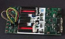
Official Atmel AVR development tools and evaluation kits contain a number of starter kits and debugging tools with support for most AVR devices:
STK600 starter kit
The STK600 starter kit and development system is an update to the STK500.[33] The STK600 uses a base board, a signal routing board, and a target board.
The base board is similar to the STK500, in that it provides a power supply, clock, in-system programming, an RS-232 port and a CAN (Controller Area Network, an automotive standard) port via DE9 connectors, and stake pins for all of the GPIO signals from the target device.
The target boards have ZIF sockets for DIP, SOIC, QFN, or QFP packages, depending on the board.
The signal routing board sits between the base board and the target board, and routes the signals to the proper pin on the device board. There are many different signal routing boards that could be used with a single target board, depending on what device is in the ZIF socket.
The STK600 allows in-system programming from the PC via USB, leaving the RS-232 port available for the target microcontroller. A 4 pin header on the STK600 labeled 'RS-232 spare' can connect any TTL level USART port on the chip to an onboard MAX232 chip to translate the signals to RS-232 levels. The RS-232 signals are connected to the RX, TX, CTS, and RTS pins on the DB-9 connector.
STK500 starter kit
The STK500 starter kit and development system features ISP and high voltage programming (HVP) for all AVR devices, either directly or through extension boards. The board is fitted with DIP sockets for all AVRs available in DIP packages.
STK500 Expansion Modules: Several expansion modules are available for the STK500 board:
- STK501 – Adds support for microcontrollers in 64-pin TQFP packages.
- STK502 – Adds support for LCD AVRs in 64-pin TQFP packages.
- STK503 – Adds support for microcontrollers in 100-pin TQFP packages.
- STK504 – Adds support for LCD AVRs in 100-pin TQFP packages.
- STK505 – Adds support for 14 and 20-pin AVRs.
- STK520 – Adds support for 14 and 20, and 32-pin microcontrollers from the AT90PWM and ATmega family.
- STK524 – Adds support for the ATmega32M1/C1 32-pin CAN/LIN/Motor Control family.
- STK525 – Adds support for the AT90USB microcontrollers in 64-pin TQFP packages.
- STK526 – Adds support for the AT90USB microcontrollers in 32-pin TQFP packages.
STK200 starter kit
The STK200 starter kit and development system has a DIP socket that can host an AVR chip in a 40, 20, or 8-pin package. The board has a 4 MHz clock source, 8 light-emitting diode (LED)s, 8 input buttons, an RS-232 port, a socket for a 32k SRAM and numerous general I/O. The chip can be programmed with a dongle connected to the parallel port.
| Chip | Flash size | EEPROM | SRAM | Frequency [MHz] |
Package |
|---|---|---|---|---|---|
| AT90S1200 | 1k | 64 | 0 | 12 | PDIP-20 |
| AT90S2313 | 2k | 128 | 128 | 10 | PDIP-20 |
| AT90S/LS2323 | 2k | 128 | 128 | 10 | PDIP-8 |
| AT90S/LS2343 | 2k | 128 | 128 | 10 | PDIP-8 |
| AT90S4414 | 4k | 256 | 256 | 8 | PDIP-40 |
| AT90S/LS4434 | 4k | 256 | 256 | 8 | PDIP-40 |
| AT90S8515 | 8k | 512 | 512 | 8 | PDIP-40 |
| AT90S/LS8535 | 8k | 512 | 512 | 8 | PDIP-40 |
AVRISP and AVRISP mkII
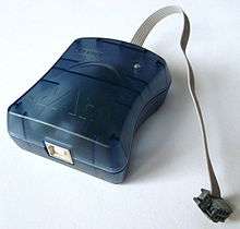
The AVRISP and AVRISP mkII are inexpensive tools allowing all AVRs to be programmed via ICSP.
The AVRISP connects to a PC via a serial port and draws power from the target system. The AVRISP allows using either of the "standard" ICSP pinouts, either the 10-pin or 6-pin connector.
The AVRISP mkII connects to a PC via USB and draws power from USB. LEDs visible through the translucent case indicate the state of target power.
As the AVRISP mkII lacks driver/buffer ICs,[34] it can have trouble programming target boards with multiple loads on its SPI lines. In such occurrences, a programmer capable of sourcing greater current is required. Alternatively, the AVRISP mkII can still be used if low-value (~150 ohm) load-limiting resistors can be placed on the SPI lines before each peripheral device.
Both the AVRISP and the AVRISP mkII are now discontinued, with product pages removed from the Microchip website. As of July 2019 the AVRISP mkII is still in stock at a number of distributors. There are also a number of 3rd party clones available.
AVR Dragon
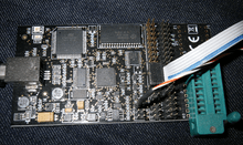
The Atmel Dragon is an inexpensive tool which connects to a PC via USB. The Dragon can program all AVRs via JTAG, HVP, PDI,[35] or ICSP. The Dragon also allows debugging of all AVRs via JTAG, PDI, or debugWire; a previous limitation to devices with 32 KB or less program memory has been removed in AVR Studio 4.18.[36] The Dragon has a small prototype area which can accommodate an 8, 28, or 40-pin AVR, including connections to power and programming pins. There is no area for any additional circuitry, although this can be provided by a third-party product called the "Dragon Rider".[37]
JTAGICE
The JTAG In Circuit Emulator (JTAGICE) debugging tool supports on-chip debugging (OCD) of AVRs with a JTAG interface. The original JTAGICE (sometimes retroactively referred to as JTAGICE mkI) uses an RS-232 interface to a PC and can only program AVR's with a JTAG interface. The JTAGICE mkI is no longer in production, however it has been replaced by the JTAGICE mkII.
JTAGICE mkII
The JTAGICE mkII debugging tool supports on-chip debugging (OCD) of AVRs with SPI, JTAG, PDI, and debugWIRE interfaces. The debugWire interface enables debugging using only one pin (the Reset pin), allowing debugging of applications running on low pin-count microcontrollers.
The JTAGICE mkII connects using USB, but there is an alternate connection via a serial port, which requires using a separate power supply. In addition to JTAG, the mkII supports ISP programming (using 6-pin or 10-pin adapters). Both the USB and serial links use a variant of the STK500 protocol.
JTAGICE3
The JTAGICE3 updates the mkII with more advanced debugging capabilities and faster programming. It connects via USB and supports the JTAG, aWire, SPI, and PDI interfaces.[38] The kit includes several adapters for use with most interface pinouts.
AVR ONE!
The AVR ONE! is a professional development tool for all Atmel 8-bit and 32-bit AVR devices with On-Chip Debug capability. It supports SPI, JTAG, PDI, and aWire programming modes and debugging using debugWIRE, JTAG, PDI, and aWire interfaces.[39]
Butterfly demonstration board
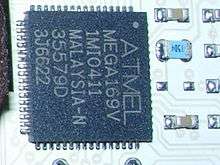
The very popular AVR Butterfly demonstration board is a self-contained, battery-powered computer running the Atmel AVR ATmega169V microcontroller. It was built to show off the AVR family, especially a then new built-in LCD interface. The board includes the LCD screen, joystick, speaker, serial port, real time clock (RTC), flash memory chip, and both temperature and voltage sensors. Earlier versions of the AVR Butterfly also contained a CdS photoresistor; it is not present on Butterfly boards produced after June 2006 to allow RoHS compliance.[40] The small board has a shirt pin on its back so it can be worn as a name badge.
The AVR Butterfly comes preloaded with software to demonstrate the capabilities of the microcontroller. Factory firmware can scroll your name, display the sensor readings, and show the time. The AVR Butterfly also has a piezoelectric transducer that can be used to reproduce sounds and music.
The AVR Butterfly demonstrates LCD driving by running a 14-segment, six alpha-numeric character display. However, the LCD interface consumes many of the I/O pins.
The Butterfly's ATmega169 CPU is capable of speeds up to 8 MHz, but it is factory set by software to 2 MHz to preserve the button battery life. A pre-installed bootloader program allows the board to be re-programmed via a standard RS-232 serial plug with new programs that users can write with the free Atmel IDE tools.
AT90USBKey
This small board, about half the size of a business card, is priced at slightly more than an AVR Butterfly. It includes an AT90USB1287 with USB On-The-Go (OTG) support, 16 MB of DataFlash, LEDs, a small joystick, and a temperature sensor. The board includes software, which lets it act as a USB mass storage device (its documentation is shipped on the DataFlash), a USB joystick, and more. To support the USB host capability, it must be operated from a battery, but when running as a USB peripheral, it only needs the power provided over USB.
Only the JTAG port uses conventional 2.54 mm pinout. All the other AVR I/O ports require more compact 1.27 mm headers.
The AVR Dragon can both program and debug since the 32 KB limitation was removed in AVR Studio 4.18, and the JTAGICE mkII is capable of both programming and debugging the processor. The processor can also be programmed through USB from a Windows or Linux host, using the USB "Device Firmware Update" protocols. Atmel ships proprietary (source code included but distribution restricted) example programs and a USB protocol stack with the device.
LUFA[41] is a third-party free software (MIT license) USB protocol stack for the USBKey and other 8-bit USB AVRs.
Raven wireless kit
The RAVEN kit supports wireless development using Atmel's IEEE 802.15.4 chipsets, for ZigBee and other wireless stacks. It resembles a pair of wireless more-powerful Butterfly cards, plus a wireless USBKey; and costing about that much (under $US100). All these boards support JTAG-based development.
The kit includes two AVR Raven boards, each with a 2.4 GHz transceiver supporting IEEE 802.15.4 (and a freely licensed ZigBee stack). The radios are driven with ATmega1284p processors, which are supported by a custom segmented LCD display driven by an ATmega3290p processor. Raven peripherals resemble the Butterfly: piezo speaker, DataFlash (bigger), external EEPROM, sensors, 32 kHz crystal for RTC, and so on. These are intended for use in developing remote sensor nodes, to control relays, or whatever is needed.
The USB stick uses an AT90USB1287 for connections to a USB host and to the 2.4 GHz wireless links. These are intended to monitor and control the remote nodes, relying on host power rather than local batteries.
Third-party programmers
A wide variety of third-party programming and debugging tools are available for the AVR. These devices use various interfaces, including RS-232, PC parallel port, and USB.[42]
Uses
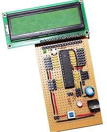
AVRs have been used in various automotive applications such as security, safety, powertrain and entertainment systems. Atmel has recently launched a new publication "Atmel Automotive Compilation" to help developers with automotive applications. Some current usages are in BMW, Daimler-Chrysler and TRW.
The Arduino physical computing platform is based on an ATmega328 microcontroller (ATmega168 or ATmega8 in board versions older than the Diecimila). The ATmega1280 and ATmega2560, with more pinout and memory capabilities, have also been employed to develop the Arduino Mega platform. Arduino boards can be used with its language and IDE, or with more conventional programming environments (C, assembler, etc.) as just standardized and widely available AVR platforms.
USB-based AVRs have been used in the Microsoft Xbox hand controllers. The link between the controllers and Xbox is USB.
Numerous companies produce AVR-based microcontroller boards intended for use by hobbyists, robot builders, experimenters and small system developers including: Cubloc,[43] gnusb,[44] BasicX,[45] Oak Micros,[46] ZX Microcontrollers,[47] and myAVR.[48] There is also a large community of Arduino-compatible boards supporting similar users.
Schneider Electric used to produce the M3000 Motor and Motion Control Chip, incorporating an Atmel AVR Core and an advanced motion controller for use in a variety of motion applications but this has been discontinued.[49]
FPGA clones
With the growing popularity of FPGAs among the open source community, people have started developing open source processors compatible with the AVR instruction set. The OpenCores website lists the following major AVR clone projects:
- pAVR,[50] written in VHDL, is aimed at creating the fastest and maximally featured AVR processor, by implementing techniques not found in the original AVR processor such as deeper pipelining.
- avr_core,[51] written in VHDL, is a clone aimed at being as close as possible to the ATmega103.
- Navré,[52] written in Verilog, implements all Classic Core instructions and is aimed at high performance and low resource usage. It does not support interrupts.
- The opencores project CPU lecture[53] written in VHDL by Dr. Jürgen Sauermann explains in detail how to design a complete AVR based System on a Chip (SoC).
Other vendors
In addition to the chips manufactured by Atmel, clones are available from LogicGreen Technologies.[54] These parts are not exact clones - they have a few features not found in the chips they are "clones" of, and higher maximum clock speeds, but use SWD instead of ISP for programming, so different programming tools must be used..
Microcontrollers using the ATmega architecture are being manufactured by NIIET in Voronezh, Russia, as part of the 1887 series of integrated circuits. This includes an ATmega128 under the designation 1887VE7T (Russian: 1887ВЕ7Т).[55]
References
- Since 1996, NTH has become part of the Norwegian University of Science and Technology (NTNU)
- alfbogen.com blog
- "The Story of AVR". youtube.com.
- "UNSW School of Computer Science and Engineering - General AVR Info". Cse.unsw.edu.au. Archived from the original on 2012-06-23. Retrieved 2012-09-19.
- An introduction to Atmel and the AVR microcontroller
- "Embedded Systems and Microcontrollers" (PDF). Archived from the original (PDF) on 2004-12-24. Retrieved 2018-10-01.
- Myklebust, Gaute. "The AVR Microcontroller and C Compiler Co-Design" (PDF). Atmel Norway. CiteSeerX 10.1.1.63.1447. Retrieved 2012-09-19.
- Atmel press release. "Atmel's AVR Microcontroller Ships 500 Million Units".
- Field Programmable System Level Integrated Circuit Archived 2012-11-27 at the Wayback Machine
- atmel.com
- Atmel Smart Card ICs
- "AVR319: Using the USI module for SPI communication" (PDF). Atmel. 2004. Retrieved 10 June 2014.
- "Atmel AVR310: Using the USI Module as a I2C Master" (PDF). Atmel. 2013. Retrieved 10 June 2014.
- "AVR312: Using the USI module as a I2C slave" (PDF). Atmel. 2005. Retrieved 10 June 2014.
- "AVR307: Half Duplex UART Using the USI Module" (PDF). Atmel. 2003. Retrieved 10 June 2014.
- "AVR Hardware Design Considerations" (PDF) (application note). Atmel Corporation. Jun 2015. p. 5. Retrieved 14 Jun 2015.
The reset line has an internal pull-up resistor, but if the environment is noisy it can be insufficient and reset can therefore occur sporadically.
- "AVRDUDE programmer". Savannah.nongnu.org. Retrieved 2012-09-19.
- "PDI programming driver" (PDF). Retrieved 2012-09-19.
- "HVSP_Description". Support.atmel.no. Archived from the original on 2009-10-12. Retrieved 2012-09-19.
- "DES-encrypted AVR Bootloader" (PDF). Retrieved 2012-09-19.
- "AES-encrypted AVR Bootloader" (PDF). Retrieved 2012-09-19.
- "XMEGA Bootloader" (PDF). Retrieved 2012-09-19.
- "AVR USB Bootloader" (PDF). Retrieved 2012-09-19.
- "Atmel's Self-Programming Flash Microcontrollers" (PDF). Retrieved 12 March 2020.
- "Guide to understanding JTAG and security fuses on the AVR". Retrieved 2012-09-19.
- "Atmel-ICE - Atmel Corporation". Atmel.com. Retrieved 2015-09-11.
- "JTAGICE 3- Atmel Corporation". Atmel.com. Retrieved 2012-09-19.
- "AVR JTAGICE mkII". Atmel. Archived from the original on 15 February 2013. Retrieved 13 January 2013.
- "JTAGICE mkII Communication Protocol" (PDF). Retrieved 2012-09-19.
- "AVR Dragon". Atmel. Retrieved 13 January 2013.
- "AVR JTAGICE mkII User's Guide" (PDF). microchip.com. Retrieved 25 March 2020.
- JTAGICE Press Release, 2004. Archived 2011-07-07 at the Wayback Machine
- "STK600". Atmel. Archived from the original on 15 February 2013. Retrieved 13 January 2013.
- "AVRISP mkII Disassembled". Archived from the original on 2014-11-08. Retrieved 2014-11-08.
- "AVR1005: Getting started with XMEGA, page 7" (PDF). Atmel. Retrieved 7 November 2011.
- "AVR Studio v4.18 Release Notes". Retrieved 2012-09-19.
- "ECROS Technology - Dragon Rider". Ecrostech.com. 2008-03-02. Retrieved 2012-09-19.
- JTAGICE3 Product Page
- AVR ONE! Product Page
- AVR Butterfly
- "LUFA (Formerly MyUSB)". Four Walled Cubicle. Retrieved 2012-09-19.
- See avrffreaks.net for a comprehensive list.
- "Comfile Technology". Comfile Technology, Inc. Retrieved 13 January 2013.
- "gnusb: Open Source USB Sensor Box". Retrieved 13 January 2013.
- "BasicX". NetMedia, Inc. Archived from the original on 23 May 2013. Retrieved 13 January 2013.
- "Welcome to Oak Micros". Oak Micros. Oak Micros. Archived from the original on 2012-10-25. Retrieved 13 January 2013.
- "ZBasic". Retrieved 13 January 2013.
- "myAVR". Laser & Co. Solutions GmbH. Retrieved 13 January 2013.
- "M3000 Motion controller on a chip". imshome.com. Schneider Electric Motion USA. Archived from the original on 2009-12-02. Retrieved 2011-08-02.
- "pAVR :: Overview". OpenCores. Retrieved 2012-09-19.
- "AVR Core :: Overview". OpenCores. Retrieved 2012-09-19.
- "Navré AVR clone (8-bit RISC) Overview". OpenCores. Retrieved 2012-09-19.
- "CPU lecture". OpenCores. Retrieved 2015-02-16.
- "LGT8F88A FLASH Microcontroller". LogicGreen Technologies. Archived from the original on 2017-08-29. Retrieved 2019-01-18, a clone of the ATmega88.
- "Микроконтроллеры" [Microcontrollers] (in Russian). Voronezh: OAO "NIIET". Archived from the original on 22 August 2017. Retrieved 22 August 2017.
Further reading
- AVR Programming: Learning to Write Software for Hardware; Elliot Williams; Maker Media; 474 pages; 2014; ISBN 978-1449355784
- Arduino: A Quick Start Guide; Maik Schmidt; Pragmatic Bookshelf; 276 pages; 2011; ISBN 978-1-934356-66-1.
- Some Assembly Required: Assembly Language Programming with the AVR Microcontroller; Timothy S Margush; CRC Press; 643 pages; 2011; ISBN 978-1439820643
- AVR Microcontroller and Embedded Systems: Using Assembly and C; Muhammad Ali Mazidi, Sarmad Naimi, Sepehr Naimi; Pearson; 792 pages; 2010; ISBN 978-0138003319.
External links
| Wikimedia Commons has media related to |
| The Wikibook Embedded Systems has a page on the topic of: Atmel AVR |
Official Website
Official Community
Other
- AVR microcontrollers at Curlie, numerous AVR links
- AVR-Libc
- Atmel AVR Serial Port Programmer
- Why you need a clock source for the AVR?
- AVR Basics - AVR guide for beginners
- Simplest AVR programmer Using LPT Port
- ATmega8 Breadboard Tutorial
- AVR DIP-Package Pinout Diagrams: ATtiny44/45/84/85, ATmega328P, ATmega644P, ATmega1284P
- AVR TQFP-Package Pinout Diagrams: ATmega328, ATmega2560, ATmega32U4
