Power MOSFET
A power MOSFET is a specific type of metal–oxide–semiconductor field-effect transistor (MOSFET) designed to handle significant power levels. Compared to the other power semiconductor devices, such as an insulated-gate bipolar transistor (IGBT) or a thyristor, its main advantages are high switching speed and good efficiency at low voltages. It shares with the IGBT an isolated gate that makes it easy to drive. They can be subject to low gain, sometimes to a degree that the gate voltage needs to be higher than the voltage under control.
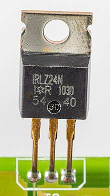
The design of power MOSFETs was made possible by the evolution of MOSFET and CMOS technology, used for manufacturing integrated circuits since the 1960s. The power MOSFET shares its operating principle with its low-power counterpart, the lateral MOSFET. The power MOSFET, which is commonly used in power electronics, was adapted from the standard MOSFET and commercially introduced in the 1970s.[2]
The power MOSFET is the most common power semiconductor device in the world, due to its low gate drive power, fast switching speed,[3] easy advanced paralleling capability,[3][4] wide bandwidth, ruggedness, easy drive, simple biasing, ease of application, and ease of repair.[4] In particular, it is the most widely used low-voltage (less than 200 V) switch. It can be found in a wide range of applications, such as most power supplies, DC-to-DC converters, low-voltage motor controllers, and many other applications.
History
The MOSFET was invented by Mohamed Atalla and Dawon Kahng at Bell Labs in 1959. It was a breakthrough in power electronics. Generations of MOSFETs enabled power designers to achieve performance and density levels not possible with bipolar transistors.[5]
In 1969, Hitachi introduced the first vertical power MOSFET,[6] which would later be known as the VMOS (V-groove MOSFET).[7] The same year, the DMOS (double-diffused MOSFET) with self-aligned gate was first reported by Y. Tarui, Y. Hayashi and Toshihiro Sekigawa of the Electrotechnical Laboratory (ETL).[8][9] In 1974, Jun-ichi Nishizawa at Tohoku University invented a power MOSFET for audio, which was soon manufactured by Yamaha Corporation for their high fidelity audio amplifiers. JVC, Pioneer Corporation, Sony and Toshiba also began manufacturing amplifiers with power MOSFETs in 1974.[10] Siliconix commercially introduced a VMOS in 1975.[7]
The VMOS and DMOS developed into what has become known as VDMOS (vertical DMOS).[10] John Moll's research team at HP Labs fabricated DMOS prototypes in 1977, and demonstrated advantages over the VMOS, including lower on-resistance and higher breakdown voltage.[7] The same year, Hitachi introduced the LDMOS (lateral DMOS), a planar type of DMOS. Hitachi was the only LDMOS manufacturer between 1977 and 1983, during which time LDMOS was used in audio power amplifiers from manufacturers such as HH Electronics (V-series) and Ashly Audio, and were used for music and public address systems.[10] With the introduction of the 2G digital mobile network in 1995, the LDMOS became the most widely used RF power amplifier in mobile networks such as 2G, 3G,[11] and 4G.[12]
Alex Lidow co-invented the HexFET, a hexagonal type of Power MOSFET, at Stanford University in 1977,[13] along with Tom Herman.[14] The HexFET was commercialized by International Rectifier in 1978.[7][14] The insulated-gate bipolar transistor (IGBT), which combines elements of both the power MOSFET and the bipolar junction transistor (BJT), was developed by Jayant Baliga at General Electric between 1977 and 1979.[15]
The superjunction MOSFET is a type of power MOSFET that uses P+ columns that penetrate the N- epitaxial layer. The idea of stacking P and N layers was first proposed by Shozo Shirota and Shigeo Kaneda at Osaka University in 1978.[16] David J. Coe at Philips invented the superjunction MOSFET with alternating p-type and n-type layers by filing a US patent in 1984 which was awarded in 1988.[17]
Applications
The power MOSFET is the most widely used power semiconductor device in the world.[3] As of 2010, the power MOSFET accounts for 53% of the power transistor market, ahead of the insulated-gate bipolar transistor (27%), RF power amplifier (11%) and bipolar junction transistor (9%).[18] As of 2018, over 50 billion power MOSFETs are shipped annually.[19] These include the trench power MOSFET, which sold over 100 billion units up until February 2017,[20] and STMicroelectronics' MDmesh (superjunction MOSFET) which has sold 5 billion units as of 2019.[16]
Power MOSFETs are commonly used for a wide range of consumer electronics.[21][22]
RF DMOS, also known as RF power MOSFET, is a type of DMOS power transistor designed for radio-frequency (RF) applications. It is used in various radio and RF applications.[23][24]
Power MOSFETs are widely used in transportation technology,[25][26][27] which include a wide range of vehicles.
In the automotive industry,[28][29][30] power MOSFETs are widely used in automotive electronics.[31][32][21]
Power MOSFETs (including DMOS, LDMOS and VMOS) are commonly used for a wide range of other applications.
Basic structure
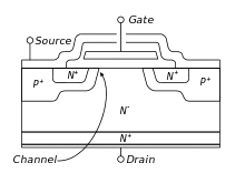
Several structures had been explored in the 1970s, when the first commercial power MOSFETs were introduced. However, most of them have been abandoned (at least until recently) in favour of the Vertical Diffused MOS (VDMOS) structure (also called Double-Diffused MOS or simply DMOS) and the LDMOS (laterally diffused MOS) structure.
The cross section of a VDMOS (see figure 1) shows the "verticality" of the device: it can be seen that the source electrode is placed over the drain, resulting in a current mainly vertical when the transistor is in the on-state. The "diffusion" in VDMOS refers to the manufacturing process: the P wells (see figure 1) are obtained by a diffusion process (actually a double diffusion process to get the P and N+ regions, hence the name double diffused).
Power MOSFETs have a different structure from the lateral MOSFET: as with most power devices, their structure is vertical and not planar. In a planar structure, the current and breakdown voltage ratings are both functions of the channel dimensions (respectively width and length of the channel), resulting in inefficient use of the "silicon real estate". With a vertical structure, the voltage rating of the transistor is a function of the doping and thickness of the N epitaxial layer (see cross section), while the current rating is a function of the channel width. This makes it possible for the transistor to sustain both high blocking voltage and high current within a compact piece of silicon.
LDMOS are power MOSFETs with a lateral structure. They are mainly used in high-end audio power amplifiers,[10] and RF power amplifiers in wireless cellular networks, such as 2G, 3G,[11] and 4G.[12] Their advantage is a better behaviour in the saturated region (corresponding to the linear region of a bipolar junction transistor) than the vertical MOSFETs. Vertical MOSFETs are designed for switching applications, so they are only used in On or Off states.
On-state resistance
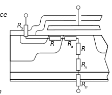
When the power MOSFET is in the on-state (see MOSFET for a discussion on operation modes), it exhibits a resistive behaviour between the drain and source terminals. It can be seen in figure 2 that this resistance (called RDSon for "drain to source resistance in on-state") is the sum of many elementary contributions:
- RS is the source resistance. It represents all resistances between the source terminal of the package to the channel of the MOSFET: resistance of the wire bonds, of the source metallisation, and of the N+ wells;
- Rch. This is the channel resistance. It is inversely proportional to the channel width, and for a given die size, to the channel density. The channel resistance is one of the main contributors to the RDSon of low-voltage MOSFETs, and intensive work has been carried out to reduce their cell size in order to increase the channel density;
- Ra is the access resistance. It represents the resistance of the epitaxial zone directly under the gate electrode, where the direction of the current changes from horizontal (in the channel) to vertical (to the drain contact);
- RJFET is the detrimental effect of the cell size reduction mentioned above: the P implantations (see figure 1) form the gates of a parasitic JFET transistor that tend to reduce the width of the current flow;
- Rn is the resistance of the epitaxial layer. As the role of this layer is to sustain the blocking voltage, Rn is directly related to the voltage rating of the device. A high voltage MOSFET requires a thick, low-doped layer, i.e., highly resistive, whereas a low-voltage transistor only requires a thin layer with a higher doping level, i.e., less resistive. As a result, Rn is the main factor responsible for the resistance of high-voltage MOSFETs;
- RD is the equivalent of RS for the drain. It represents the resistance of the transistor substrate (the cross section in figure 1 is not at scale, the bottom N+ layer is actually the thickest) and of the package connections.
Breakdown voltage/on-state resistance trade-off

When in the OFF-state, the power MOSFET is equivalent to a PIN diode (constituted by the P+ diffusion, the N− epitaxial layer and the N+ substrate). When this highly non-symmetrical structure is reverse-biased, the space-charge region extends principally on the light-doped side, i.e., over the N− layer. This means that this layer has to withstand most of the MOSFET's OFF-state drain-to-source voltage.
However, when the MOSFET is in the ON-state, this N− layer has no function. Furthermore, as it is a lightly doped region, its intrinsic resistivity is non-negligible and adds to the MOSFET's ON-state Drain-to-Source Resistance (RDSon) (this is the Rn resistance in figure 2).
Two main parameters govern both the breakdown voltage and the RDSon of the transistor: the doping level and the thickness of the N− epitaxial layer. The thicker the layer and the lower its doping level, the higher the breakdown voltage. On the contrary, the thinner the layer and the higher the doping level, the lower the RDSon (and therefore the lower the conduction losses of the MOSFET). Therefore, it can be seen that there is a trade-off in the design of a MOSFET, between its voltage rating and its ON-state resistance. This is demonstrated by the plot in figure 3.
Body diode
It can be seen in figure 1 that the source metallization connects both the N+ and P+ implantations, although the operating principle of the MOSFET only requires the source to be connected to the N+ zone. However, if it were, this would result in a floating P zone between the N-doped source and drain, which is equivalent to a NPN transistor with a non-connected base. Under certain conditions (under high drain current, when the on-state drain to source voltage is in the order of some volts), this parasitic NPN transistor would be triggered, making the MOSFET uncontrollable. The connection of the P implantation to the source metallization shorts the base of the parasitic transistor to its emitter (the source of the MOSFET) and thus prevents spurious latching.
This solution, however, creates a diode between the drain (cathode) and the source (anode) of the MOSFET, making it able to block current in only one direction.
Body diodes may be utilized as freewheeling diodes for inductive loads in configurations such as H bridge or half bridge. While these diodes usually have rather high forward voltage drop, they can handle large currents and are sufficient in many applications, reducing part count, and thus, device cost and board space.
Switching operation

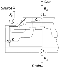
Because of their unipolar nature, the power MOSFET can switch at very high speed. Indeed, there is no need to remove minority carriers as with bipolar devices. The only intrinsic limitation in commutation speed is due to the internal capacitances of the MOSFET (see figure 4). These capacitances must be charged or discharged when the transistor switches. This can be a relatively slow process because the current that flows through the gate capacitances is limited by the external driver circuit. This circuit will actually dictate the commutation speed of the transistor (assuming the power circuit has sufficiently low inductance).
Capacitances
In the MOSFET datasheets, the capacitances are often named Ciss (input capacitance, drain and source terminal shorted), Coss (output capacitance, gate and source shorted), and Crss (reverse transfer capacitance, source connected to ground). The relationship between these capacitances and those described below is:
Where CGS, CGD and CDS are respectively the gate-to-source, gate-to-drain and drain-to-source capacitances (see below). Manufacturers prefer to quote Ciss, Coss and Crss because they can be directly measured on the transistor. However, as CGS, CGD and CDS are closer to the physical meaning, they will be used in the remaining of this article.
Gate to source capacitance
The CGS capacitance is constituted by the parallel connection of CoxN+, CoxP and Coxm (see figure 4). As the N+ and P regions are highly doped, the two former capacitances can be considered as constant. Coxm is the capacitance between the (polysilicon) gate and the (metal) source electrode, so it is also constant. Therefore, it is common practice to consider CGS as a constant capacitance, i.e. its value does not depend on the transistor state.
Gate to drain capacitance
The CGD capacitance can be seen as the connection in series of two elementary capacitances. The first one is the oxide capacitance (CoxD), constituted by the gate electrode, the silicon dioxide and the top of the N epitaxial layer. It has a constant value. The second capacitance (CGDj) is caused by the extension of the space-charge zone when the MOSFET is in off-state. Therefore, it is dependent upon the drain to source voltage. From this, the value of CGD is:
The width of the space-charge region is given by[33]
where is the permittivity of the Silicon, q is the electron charge, and N is the doping level. The value of CGDj can be approximated using the expression of the plane capacitor:
Where AGD is the surface area of the gate-drain overlap. Therefore, it comes:
It can be seen that CGDj (and thus CGD) is a capacitance which value is dependent upon the gate to drain voltage. As this voltage increases, the capacitance decreases. When the MOSFET is in on-state, CGDj is shunted, so the gate to drain capacitance remains equal to CoxD, a constant value.
Drain to source capacitance
As the source metallization overlaps the P-wells (see figure 1), the drain and source terminals are separated by a P-N junction. Therefore, CDS is the junction capacitance. This is a non-linear capacitance, and its value can be calculated using the same equation as for CGDj.
Other dynamic elements
Packaging inductances
To operate, the MOSFET must be connected to the external circuit, most of the time using wire bonding (although alternative techniques are investigated). These connections exhibit a parasitic inductance, which is in no way specific to the MOSFET technology, but has important effects because of the high commutation speeds. Parasitic inductances tend to maintain their current constant and generate overvoltage during the transistor turn off, resulting in increasing commutation losses.
A parasitic inductance can be associated with each terminal of the MOSFET. They have different effects:
- the gate inductance has little influence (assuming it is lower than some hundreds of nanohenries), because the current gradients on the gate are relatively slow. In some cases, however, the gate inductance and the input capacitance of the transistor can constitute an oscillator. This must be avoided, as it results in very high commutation losses (up to the destruction of the device). On a typical design, parasitic inductances are kept low enough to prevent this phenomenon;
- the drain inductance tends to reduce the drain voltage when the MOSFET turns on, so it reduces turn on losses. However, as it creates an overvoltage during turn-off, it increases turn-off losses;
- the source parasitic inductance has the same behaviour as the drain inductance, plus a feedback effect that makes commutation last longer, thus increasing commutation losses.
- at the beginning of a fast turn-on, due to the source inductance, the voltage at the source (on the die) will be able to jump up as well as the gate voltage; the internal VGS voltage will remain low for a longer time, therefore delaying turn-on.
- at the beginning of a fast turn-off, as current through the source inductance decreases sharply, the resulting voltage across it goes negative (with respect to the lead outside the package) raising the internal VGS voltage, keeping the MOSFET on, and therefore delaying turn-off.
Limits of operation
Gate oxide breakdown
The gate oxide is very thin (100 nm or less), so it can only sustain a limited voltage. In the datasheets, manufacturers often state a maximum gate to source voltage, around 20 V, and exceeding this limit can result in destruction of the component. Furthermore, a high gate to source voltage reduces significantly the lifetime of the MOSFET, with little to no advantage on RDSon reduction.
To deal with this issue, a gate driver circuit is often used.
Maximum drain to source voltage
Power MOSFETs have a maximum specified drain to source voltage (when turned off), beyond which breakdown may occur. Exceeding the breakdown voltage causes the device to conduct, potentially damaging it and other circuit elements due to excessive power dissipation.
Maximum drain current
The drain current must generally stay below a certain specified value (maximum continuous drain current). It can reach higher values for very short durations of time (maximum pulsed drain current, sometimes specified for various pulse durations). The drain current is limited by heating due to resistive losses in internal components such as bond wires, and other phenomena such as electromigration in the metal layer.
Maximum temperature
The junction temperature (TJ) of the MOSFET must stay under a specified maximum value for the device to function reliably, determined by MOSFET die layout and packaging materials. The packaging often limits the maximum junction temperature, due to the molding compound and (where used) epoxy characteristics.
The maximum operating ambient temperature is determined by the power dissipation and thermal resistance. The junction-to-case thermal resistance is intrinsic to the device and package; the case-to-ambient thermal resistance is largely dependent on the board/mounting layout, heatsinking area and air/fluid flow.
The type of power dissipation, whether continuous or pulsed, affects the maximum operating temperature, due to thermal mass characteristics; in general, the lower the frequency of pulses for a given power dissipation, the higher maximum operating ambient temperature, due to allowing a longer interval for the device to cool down. Models, such as a Foster network, can be used to analyze temperature dynamics from power transients.
Safe operating area
The safe operating area defines the combined ranges of drain current and drain to source voltage the power MOSFET is able to handle without damage. It is represented graphically as an area in the plane defined by these two parameters. Both drain current and drain-to-source voltage must stay below their respective maximum values, but their product must also stay below the maximum power dissipation the device is able to handle. Thus, the device cannot be operated at its maximum current and maximum voltage simultaneously.[34]
Latch-up
The equivalent circuit for a power MOSFET consists of one MOSFET in parallel with a parasitic BJT. If the BJT turns ON, it cannot be turned off, since the gate has no control over it. This phenomenon is known as "latch-up", which can lead to device destruction. The BJT can be turned on due to a voltage drop across the p-type body region. To avoid latch-up, the body and the source are typically short-circuited within the device package.
Technology

Layout
Cellular structure
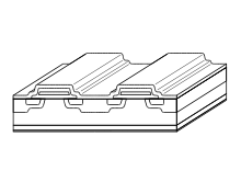
As described above, the current handling capability of a power MOSFET is determined by its gate channel width. The gate channel width is the third (Z-axis) dimension of the cross-sections pictured.
To minimize cost and size, it is valuable to keep the transistor's die area size as small as possible. Therefore, optimizations have been developed to increase the width of the channel surface area, i.e., increase the "channel density". They mainly consist of creating cellular structures repeated over the whole area of the MOSFET die. Several shapes have been proposed for these cells, the most famous being the hexagonal shape used in International Rectifier's HEXFET® devices.
Another way to increase the channel density is to reduce the size of the elementary structure. This allows for more cells in a given surface area, and therefore more channel width. However, as the cell size shrinks, it becomes more difficult to ensure proper contact of every cell. To overcome this, a "strip" structure is often used (see figure). It is less efficient than a cellular structure of equivalent resolution in terms of channel density, but can cope with smaller pitch. Another advantage of the planar stripe structure is that it is less susceptible to failure during avalanche breakdown events in which the parasitic bipolar transistor turns on from sufficient forward bias. In the cellular structure, if the source terminal of any one cell is poorly contacted, then it becomes much more likely that the parasitic bipolar transistor latches on during an avalanche breakdown event. Because of this, MOSFETs utilizing a planar stripe structure can only fail during avalanche breakdown due to extreme thermal stress.[35]
Structures


P-substrate power MOSFET
A P-substrate MOSFET (often called PMOS) is a MOSFET with opposite doping types (N instead of P and P instead of N in the cross-section in figure 1). This MOSFET is made using a P-type substrate, with a P− epitaxy. As the channel sits in a N-region, this transistor is turned on by a negative gate to source voltage. This makes it desirable in a buck converter, where one of the terminals of the switch is connected to the high side of the input voltage: with a N-MOSFET, this configuration requires to apply to the gate a voltage equal to , whereas no voltage over is required with a P-MOSFET.
The main disadvantage of this type of MOSFET is the poor on-state performance, as it uses holes as charge carriers, which have a much lower mobility than electrons. As resistivity is directly related to mobility, a given PMOS device will have a three times higher than a N-MOSFET with the same dimensions.
VMOS
The VMOS structure has a V-groove at the gate region and was used for the first commercial devices.[36]
UMOS

In this power MOSFET structure, also called trench-MOS, the gate electrode is buried in a trench etched in the silicon. This results in a vertical channel. The main interest of the structure is the absence of the JFET effect. The name of the structure comes from the U-shape of the trench.
Super-junction deep-trench technology
Especially for voltages beyond 500 V, some manufacturers, including Infineon Technologies with its CoolMOS™ products, have begun to use a charge compensation principle. With this technology, the resistance of the epitaxial layer, which is the biggest contributor (more than 95%) to the device resistance of high-voltage MOSFETs, can be reduced by a factor of greater than 5.
Seeking to improve the manufacturing efficiency and reliability of super-junction MOSFETs, Renesas Electronics developed a super-junction structure with a deep-trench process technique. This technology entails etching trenches in the low-impurity N-type material to form P-type regions. This process overcomes problems inherent to the multi-level epitaxial growth approach and results in extremely low on-resistance and reduced internal capacitance.
Due to the increased p-n junction area, a super-junction structure has a smaller reverse recovery time but larger reverse recovery current compared to a conventional planar power MOSFET.
References
- IRLZ24N, 55V N-Channel Power MOSFET, TO-220AB package; Infineon.
- Irwin, J. David (1997). The Industrial Electronics Handbook. CRC Press. p. 218. ISBN 9780849383434.
- "Power MOSFET Basics" (PDF). Alpha & Omega Semiconductor. Retrieved 29 July 2019.
- Duncan, Ben (1996). High Performance Audio Power Amplifiers. Elsevier. pp. 178–81. ISBN 9780080508047.
- "Rethink Power Density with GaN". Electronic Design. 21 April 2017. Retrieved 23 July 2019.
- Oxner, E. S. (1988). Fet Technology and Application. CRC Press. p. 18. ISBN 9780824780500.
- "Advances in Discrete Semiconductors March On". Power Electronics Technology. Informa: 52–6. September 2005. Archived (PDF) from the original on 22 March 2006. Retrieved 31 July 2019.
- Tarui, Y.; Hayashi, Y.; Sekigawa, Toshihiro (September 1969). "Diffusion Self-Aligned MOST; A New Approach for High Speed Device". Proceedings of the 1st Conference on Solid State Devices. doi:10.7567/SSDM.1969.4-1.
- McLintock, G. A.; Thomas, R. E. (December 1972). "Modelling of the double-diffused MOST's with self-aligned gates". 1972 International Electron Devices Meeting: 24–26. doi:10.1109/IEDM.1972.249241.
- Duncan, Ben (1996). High Performance Audio Power Amplifiers. Elsevier. pp. 177–8, 406. ISBN 9780080508047.
- Baliga, B. Jayant (2005). Silicon RF Power MOSFETS. World Scientific. ISBN 9789812561213.
- Asif, Saad (2018). 5G Mobile Communications: Concepts and Technologies. CRC Press. p. 134. ISBN 9780429881343.
- "SEMI Award for North America". SEMI. Archived from the original on 5 August 2016. Retrieved 5 August 2016.
- "International Rectifier's Alex Lidow and Tom Herman Inducted Into Engineering Hall of Fame". Business Wire. 14 September 2004. Retrieved 31 July 2019.
- Baliga, B. Jayant (2015). The IGBT Device: Physics, Design and Applications of the Insulated Gate Bipolar Transistor. William Andrew. pp. xxviii, 5–11. ISBN 9781455731534.
- "MDmesh: 20 Years of Superjunction STPOWER™ MOSFETs, A Story About Innovation". STMicroelectronics. 11 September 2019. Retrieved 2 November 2019.
- US Patent 4,754,310
- "Power Transistor Market Will Cross $13.0 Billion in 2011". IC Insights. June 21, 2011. Retrieved 15 October 2019.
- Carbone, James (September–October 2018). "Buyers can expect 30-week lead times and higher tags to continue for MOSFETs" (PDF). Electronics Sourcing: 18–19.
- Williams, Richard K.; Darwish, Mohamed N.; Blanchard, Richard A.; Siemieniec, Ralf; Rutter, Phil; Kawaguchi, Yusuke (23 February 2017). "The Trench Power MOSFET: Part I—History, Technology, and Prospects". IEEE Transactions on Electron Devices. 64 (3): 674–691. Bibcode:2017ITED...64..674W. doi:10.1109/TED.2017.2653239.
- "MOSFET". Infineon Technologies. Retrieved 24 December 2019.
- "Infineon EiceDRIVER™ gate driver ICs" (PDF). Infineon. August 2019. Retrieved 26 December 2019.
- "RF DMOS Transistors". STMicroelectronics. Retrieved 22 December 2019.
- "AN1256: Application note – High-power RF MOSFET targets VHF applications" (PDF). ST Microelectronics. July 2007. Retrieved 22 December 2019.
- Emadi, Ali (2017). Handbook of Automotive Power Electronics and Motor Drives. CRC Press. p. 117. ISBN 9781420028157.
- "Infineon Solutions for Transportation" (PDF). Infineon. June 2013. Retrieved 23 December 2019.
- "HITFETs: Smart, Protected MOSFETs" (PDF). Infineon. Retrieved 23 December 2019.
- "CMOS Sensors Enable Phone Cameras, HD Video". NASA Spinoff. NASA. Retrieved 6 November 2019.
- Veendrick, Harry J. M. (2017). Nanometer CMOS ICs: From Basics to ASICs. Springer. p. 245. ISBN 9783319475974.
- Korec, Jacek (2011). Low Voltage Power MOSFETs: Design, Performance and Applications. Springer Science+Business Media. pp. 9–14. ISBN 978-1-4419-9320-5.
- "Automotive Power MOSFETs" (PDF). Fuji Electric. Retrieved 10 August 2019.
- Williams, R. K.; Darwish, M. N.; Blanchard, R. A.; Siemieniec, R.; Rutter, P.; Kawaguchi, Y. (2017). "The Trench Power MOSFET—Part II: Application Specific VDMOS, LDMOS, Packaging, Reliability". IEEE Transactions on Electron Devices. 64 (3): 692–712. Bibcode:2017ITED...64..692W. doi:10.1109/TED.2017.2655149. ISSN 0018-9383.
- Simon M. Sze, Modern semiconductor device physics, John Wiley and Sons, Inc 1998 ISBN 0-471-15237-4
- Pierre Aloïsi, Les transistors MOS de puissance in Interrupteurs électroniques de puissance, traite EGEM, under the direction of Robert Perret, Lavoisier, Paris, 2003 [in French] ISBN 2-7462-0671-4
- http://www.irf.com/technical-info/whitepaper/pcim2000.pdf
- Duncan A. Grant, John Gowar POWER MOSFETS: Theory and Applications John Wiley and Sons, Inc ISBN 0-471-82867-X , 1989
Further reading
- "Power Semiconductor Devices", B. Jayant Baliga, PWS publishing Company, Boston. ISBN 0-534-94098-6