STEbus
The STEbus (also called the IEEE-1000 bus[1]) is a non-proprietary, processor-independent, computer bus with 8 data lines and 20 address lines. It was popular for industrial control systems in the late 1980s and early 1990s before the ubiquitous IBM PC dominated this market.


It remains a well-designed standard. Although no longer competitive in its original market, it is valid choice for hobbyists wishing to make 'home brew' computer systems. The Z80 and probably the CMOS 65C02 would be good processors to use. The standardized bus would allow hobbyists to interface to each other's designs.
Origins
In the early 1980s there were many proprietary bus systems, each with its own strengths and weaknesses. Most had grown in an ad-hoc manner, typically around a particular microprocessor. The S-100 bus is based on Intel 8080 signals, the STD Bus around Z80 signals, the SS-50 Bus around the Motorola 6800, and the G64 bus around 68000 signals.
This made it harder to interface other processors. Upgrading to a more powerful processor would subtly change the timings, and timing restraints were not always tightly specified. Nor were electrical parameters and physical dimensions. They usually used edge-connectors for the bus, which were vulnerable to dirt and vibration.
The VMEbus had provided a high-quality solution for high-performance 16-bit processors, using reliable DIN 41612 connectors and well-specified Eurocard board sizes and rack systems. However, these were too costly where an application only needed a modest 8-bit processor.
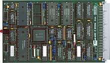
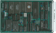
In the mid 1980s the STEbus standard addressed these issues by specifying what is rather like a VMEbus simplified for 8-bit processors. The bus signals are sufficiently generic so that they are easy for 8-bit processors to interface with. The board size was usually a single-height Eurocard (100 mm x 160 mm) but allowed for double-height boards (233 x 160 mm) as well.[2] The latter positioned the bus connector so that it could neatly merge into VME-bus systems.
IEEE Working Group P1000 initially considered simply repinning the STD Bus, replacing its card edge connector with the DIN41612 connector. But they decided to create a completely new high-performance 8-bit bus. They decided to make a bus more like the VMEbus and Futurebus. The STEbus was designed to be manufacturer independent, processor independent, and have multimaster capability. [3]
Maturity
The STEbus was very successful in its day. It was given the official standard IEEE1000-1987.
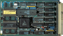
Many processors were available on STEbus cards, across a range of price and performance. These boards included the Intel 8031, 8085, 8088, 80188; the National Semiconductor 32008 and 32016; the Motorola 6809, 68000, and 68008; The Zilog Z80 and Z280; the Hitachi HD64180; and the Inmos Transputer.[3]
The STEbus is designed for 8-bit microprocessors. Processors that normally use a wider data bus (16-bit, etc.) can use the STEbus if the processor can handle data in byte-wide chunks, giving the slave as long as it needs to respond.[1]
The STEbus supported processors from the popular Z80, the 6809, to the powerful 68020. The only popular micro notably absent was the 6502, because it did not naturally support wait-states while writing. The CMOS 65C02 did not have this shortcoming, but this was rarer and more expensive than the NMOS 6502 and Z80. The 6809 used cycle stretching.
Peripheral boards included prototyping boards, disc controllers, video cards, serial I/O, analogue and digital I/O. The STEbus achieved its goal of providing a rack-mounting system robust enough for industrial use, with easily interchangeable boards and processor independence. [4]
Researchers describe STEbus systems as rugged, adaptable, and cost effective.[5]
Decline
The STEbus market began to decline as the IBM PC made progress into industrial control systems. Customers opted for PC-based products as the software base was larger and cheaper. More programmers were familiar with the PC and did not have to learn new systems.
Memory costs fell, so there was less reason to have bus-based memory expansion when one could have plenty on the processor board.
So despite the disadvantages, manufacturers created industrial PC systems and eventually dropped other bus systems.
Moving on, PC systems did away with the need for card cages and backplanes by moving to the PC104 format where boards stack onto each other. While not as well designed as the STEbus, PC104 is good enough for many applications.
The major manufacturers from its peak period now support STEbus mostly for goodwill with old customers who bought a lot of product from them.
As of 2013, some manufacturers still support STEbus, G64, Multibus II, and other legacy bussed systems.[6]
The IEEE have withdrawn the standard, not because of any faults but because it is no longer active enough to update.
Physical format
3U Eurocard - The most common size was the 100 x 160 mm Eurocard.
6U Eurocard - Rare, sometimes used in VMEbus hybrid boards
Connector
DIN 41612, rows a and c, 0.1" pitch.
VME/STE hybrid boards have the STEbus and VMEbus sharing the VME P2 connector, VME signals on row b. For this reason, STEbus boards may not use row b for any purpose.
Pinout
| num. | name | a b c | name |
|---|---|---|---|
| 1 | GND | o + o | GND |
| 2 | +5V | o + o | +5V |
| 3 | D0 | o + o | D1 |
| 4 | D2 | o + o | D3 |
| 5 | D4 | o + o | D5 |
| 6 | D6 | o + o | D7 |
| 7 | A0 | o + o | GND |
| 8 | A2 | o + o | A1 |
| 9 | A4 | o + o | A3 |
| 10 | A6 | o + o | A5 |
| 11 | A8 | o + o | A7 |
| 12 | A10 | o + o | A9 |
| 13 | A12 | o + o | A11 |
| 14 | A14 | o + o | A13 |
| 15 | A16 | o + o | A15 |
| 16 | A18 | o + o | A17 |
| 17 | CM0 | o + o | A19 |
| 18 | CM2 | o + o | CM1 |
| 19 | ADRSTB* | o + o | GND |
| 20 | DATACK* | o + o | DATSTB* |
| 21 | TRFERR* | o + o | GND |
| 22 | ATNRQ0* | o + o | SYSRST* |
| 23 | ATNRQ2* | o + o | ATNRQ1* |
| 24 | ATNRQ4* | o + o | ATNRQ3* |
| 25 | ATNRQ6* | o + o | ATNRQ5* |
| 26 | GND | o + o | ATNRQ7* |
| 27 | BUSRQ0* | o + o | BUSRQ1* |
| 28 | BUSAK0* | o + o | BUSAK1* |
| 29 | SYSCLK | o + o | VSTBY |
| 30 | -12V | o + o | +12V |
| 31 | +5V | o + o | +5V |
| 32 | GND | o + o | GND |
Active low signals indicated by asterisk.
GND: Ground reference voltage
+5V: Powers most logic.
+12V and -12V: Primarily useful for RS232 buffer power. The +12V has been used for programming voltage generators. Both can be used in analogue circuitry, but note that these are primarily power rails for digital circuitry and as such they often have digital noise. Some decoupling or local regulation is recommended for analogue circuitry.
VSTBY: Standby voltage. Optional. This line is reserved for carrying a battery backup voltage to boards that supply or consume it. A 3.6V NiCad battery is a common source. The STEbus spec is not rigid about where this should be sourced from.
In practice, this means that most boards requiring backup power tend to play safe and have a battery on board, often with a link to allow it to supply or accept power from VSTBY. Hence you can end up with more batteries in your system than you need, and you must then take care that no more than one battery is driving VSTBY.
D0...7: Data bus. This is only 8-bits wide, but most I/O or memory-mapped peripherals are byte-oriented.
A0...19: Address bus. This allows up to 1 MByte of memory to be addressed. Current technology is such that processor requiring large amounts of memory have this on the processor board, so this is not a great limitation. I/O space is limited to 4K, to simplify I/O address decoding to a practical level. A single 74LS688 on each slave board can decode A11...A4 to locate I/O slave boards at any I/O address with 16-byte alignment.[1][7] Typically 8 small jumpers or a single unit of 8 DIP switches or two binary-coded hexadecimal rotary switches are used to give each I/O slave board a unique address.[1]
CM0...2: Command Modifiers. These indicate the nature of the data transfer cycle.
| CM 2 1 0 |
Function | |
|---|---|---|
| 1 1 1 | read | memory |
| 1 1 0 | write | |
| 1 0 1 | read | I/O |
| 1 0 0 | write | |
| 0 1 1 | acknowledge | |
| 0 1 0 | reserved | |
| 0 0 1 | ||
| 0 0 0 | ||
A simple processor board can ignore the acknowledge state and drive CM2 high for all bus access, drive CM1 from a memory/not_IO signal, and CM0 from a read/not_write signal.
ATNRQ0...7*: Attention Requests. These are reserved for boards to signal for processor attention, a term which covers Interrupts and Direct Memory Access (DMA). The wise choice of signal does not commit these lines to being specific types, such as maskable interrupts, non-maskable interrupts, or DMA.
The number of Attention Requests reflects the intended role of the STEbus, in real-time control systems. Eight lines can be priority encoded into three bits, and is a reasonably practical number of lines to handle.
BUSRQ0...1* and BUSAK0...1*: Bus Requests and Bus Acknowledge. Optional. Used by multi-master systems.
The number of Attention Requests reflects that the STEbus aims to be simple. Single-master systems are the norm, but these signals allow systems to have secondary bus masters if needed.
DATSTB*: Data Strobe. This is the primary signal in data transfer cycles.
DATACK*: Data Acknowledge. A slave will assert this signal when to acknowledge the safe completion of a data transfer via the STEbus. This allows STEbus systems to use plug-in cards with a wide variety of speeds, an improvement on earlier bus systems that require everything to run at the speed of the slowest device.
TRFERR*: Transfer Error. A slave will assert this signal when acknowledging the erroneous completion of a data transfer via the STEbus.
ADRSTB*: Address Strobe. This signal indicates the address bus is valid. Originally, this had some practical use in DRAM boards which could start strobing the address lines into DRAM chips before the data bus was ready. The STEbus spec was later firmed up to say that slaves were not allowed to start transfers until DATSTB* was ready, so ADRSTB* has become quite redundant. Nowadays, STEbus masters can simply generate DATSTB* and ADRSTB* from the same logic signal. Slaves simply note when DATSTB* is valid (since the bus definition insists that the address will also be valid at the same time as the data. ADRSTB* also allows a bus master to retain ownership of the bus during indivisible read-modify-write cycles, by remaining active during two DATSTB* pulses. The sequence matches that of the 68008's bus. Other CPUs may require additional logic to create read-modify-write cycles.
SYSCLK: System Clock. Fixed at 16 MHz. 50% duty cycle.
SYSRST*: System Reset. [8]
The backplane connects all the DIN connectors in parallel. So a STEbus expansion card sees the same signals no matter which slot of the backplane it is plugged into.[7]
Technical notes
- Signal inputs must be Schmitt trigger
- Signal outputs must have a fanout of 20
- Backplane can have up to 21 sockets
- Active bus-termination recommended (270R pull-up to 2.8V)
- 7400 series chips are often used to build custom control boards, directly connected to the STEbus.[7]
External links
- STEbus (IEEE1000) standard (available to subscribers and IEEE members) 8. 1988. doi:10.1109/IEEESTD.1988.122133. ISBN 0-7381-4593-9.
- STEbus (ISO/IEC 10859:1997) cost: 192 Swiss francs
References
- Michael J. Spinks. "Microprocessor System Design: A Practical Introduction". 2013. p. 158, 162, 166.
- Leroy Davis. "STEBus".
- ISO/IEC 10859: 8-bit backplane interface: STEbus and mechanical core specifications for microcomputers. 1997. p. 4
- Tooley, Michael H (1995-03-17). PC-based instrumentation and control. pp. 91–101. ISBN 0-7506-2093-5.
- Prof. M. M. Cusack and Mr. J. Thomas. "Control software and hardware for a wall climbing robot". 1994.
- "Backplanes & Extender Boards: Multibus / STEbus / G64".
- Paul Qualtrough. "STEbus-based Hardware for a Model Railway Control System". 1998.
- STE bus information
- R.J. Mitchell "Microcomputer Systems Using the STE Bus" 1989