Quantum well
A quantum well is a potential well with only discrete energy values.
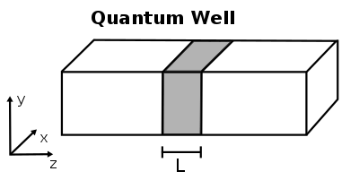
The classic model used to demonstrate a quantum well is to confine particles, which were initially free to move in three dimensions, to two dimensions, by forcing them to occupy a planar region. The effects of quantum confinement take place when the quantum well thickness becomes comparable to the de Broglie wavelength of the carriers (generally electrons and holes), leading to energy levels called "energy subbands", i.e., the carriers can only have discrete energy values.
A wide variety of electronic quantum well devices have been developed based on the theory of quantum well systems. These devices have found applications in lasers, photodetectors, modulators, and switches for example. Compared to conventional devices, quantum well devices are much faster and operate much more economically and are a point of incredible importance to the technological and telecommunication industries. These quantum well devices are currently replacing many, if not all, conventional electrical components in many electronic devices.[2]
History
The semiconductor quantum well was developed in 1970 By Esaki and Tsu, who also invented synthetic superlattices.[3] They suggested that a heterostructure made up of alternating thin layers of semiconductors with different band-gaps should exhibit interesting and useful properties.[4] Since then, much effort and research has gone into studying the physics of quantum well systems as well as developing quantum well devices.
The development of quantum well devices is greatly attributed to the advancements in crystal growth techniques. This is because quantum well devices require structures that are of high purity with few defects. Therefore, having great control over the growth of these heterostructures allows for the development of semiconductor devices that can have very fine-tuned properties.[3]
Quantum wells and semiconductor physics has been a hot topic in physics research. Development of semiconductor devices using structures made up of multiple semiconductors resulted in Nobel Prizes for Zhores Alferov and Herbert Kroemer in 2000.[5]
The theory surrounding quantum well devices has led to significant advancements in the production and efficiency of many modern components such as light-emitting diodes, transistors for example. Today, such devices are ubiquitous in modern cell phones, computers, and many other computing devices.
Fabrication
Quantum wells are formed in semiconductors by having a material, like gallium arsenide, sandwiched between two layers of a material with a wider bandgap, like aluminum arsenide. (Other examples: a layer of indium gallium nitride sandwiched between two layers of gallium nitride.) These structures can be grown by molecular beam epitaxy or chemical vapor deposition with control of the layer thickness down to monolayers.
Thin metal films can also support quantum well states, in particular, thin metallic overlayers grown in metal and semiconductor surfaces. The vacuum-metal interface confines the electron (or hole) on one side, and in general, by an absolute gap with semiconductor substrates, or by a projected band-gap with metal substrates.
There are 3 main approaches to growing a QW material system: lattice-matched, strain-balanced, and strained.[6]
- Lattice-Matched System: In a lattice-matched system, the well and the barrier have a similar lattice constant as the underlying substrate material.[6] With this method, the bandgap difference there is minimal dislocation but also a minimal shift in the absorption spectrum.
- Strain-Balanced System: In a strain-balanced system, the well and barrier are grown so that the increase in lattice constant of one of the layers is compensated by the decrease in lattice constant in the next compared to the substrate material. The choice of thickness and composition of the layers affect bandgap requirements and carrier transport limitations. This approach provides the most flexibility in design, offering a high number of periodic QWs with minimal strain relaxation.[6]
- Strained System: A strained system is grown with wells and barriers that are not similar in lattice constant. A strained system compresses the whole structure. As a result, the structure is only able to accommodate a few quantum wells.[6]
Description and overview
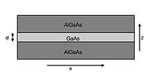
One of the simplest quantum well systems can be constructed by inserting a thin layer one type of semiconductor material between two layers of another with a different band-gap. Consider, as an example, two layers of AlGaAs with a large bandgap surrounding a thin layer of GaAs with a smaller band-gap. Let’s assume that the change in material occurs along the z-direction and therefore the potential well is along the z-direction (no confinement in the x-y plane.). Since the bandgap of the contained material is lower than the surrounding AlGaAs, a quantum well (Potential well) is created in the GaAs region. This change in band energy across the structure can be seen as the change in the potential that a carrier would feel, therefore low energy carriers can be trapped in these wells. [5]
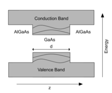
Within the quantum well, there are discrete energy eigenstates that carriers can have. For example, an electron in the conduction band can have lower energy within the well then it could have in the AlGaAs region of this structure. Consequently, an electron in the conduction band with low energy can be trapped within the quantum well. Similarly, holes in the valence band can also be trapped in the top of potential wells created in the valence band. The states that confined carriers can be in are particle-in-a-box like states.[3]
Physics
Quantum wells and quantum well devices are a subfield of solid-state physics that is still extensively studied and researched today. The theory used to describe such systems utilizes important results from the fields of quantum physics, statistical physics, and electrodynamics.
Infinite well model
The simplest model of a quantum well system is the infinite well model. The walls/barriers of the potential well are assumed to be infinite in this model. This approximation is rather unrealistic, as the potential wells created in quantum wells are generally of the order of a few hundred milli-electronvolts, which is far smaller than the infinitely high potential assumed. However, as a first approximation, the infinite well model serves as a simple and useful model that provides some insight into the physics behind quantum wells.[3]
Consider an infinite quantum well oriented in the z-direction, such that carriers in the well are confined in the z-direction but free to move in the x-y plane. we choose the quantum well to run from z = 0 to z = d. We assume that carriers experience no potential within the well and that the potential in the barrier region is infinitely high.
The Schrodinger equation for carriers in the infinite well model is:
where ħ is Planck's constant divided by 2π and m*w is the effective mass of the carriers within the well region. The effective mass of a carrier is the mass that the electron ‘feels’ in its quantum environment and generally differs between different semiconductors as the value of effective mass depends heavily on the curvature of the band. Note that m*w can be the effective mass of electrons in a well in the conduction band or for holes in a well in the valence band.
Solutions and energy levels
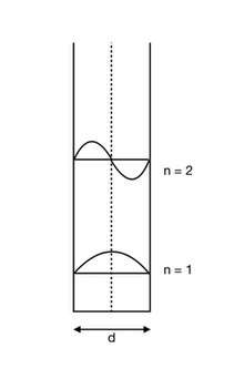
The solution wave functions cannot exist in the barrier region of the well, due to the infinitely high potential. Therefore, by imposing the following boundary conditions, the allowed wave functions are obtained,
.
The solution wave functions take the following form:
, .
The subscript n, (n>0) denotes the integer quantum number and kn is the wave vector associated with each state, given above. The associated discrete energies are given by:
.
The simple infinite well model provides a good starting point for analyzing the physics of quantum well systems and the effects of quantum confinement. The model correctly predicts that the energies in the well are inversely proportional to the square of the length of the well. This means that precise control over the width of the semiconductor layers, i.e. the length of the well, will allow for precise control of the energy levels allowed for carriers in the wells. This is an incredibly useful property for band-gap engineering. Furthermore, the model shows that the energy levels are proportional to the inverse of the effective mass. Consequently, heavy holes and light holes will have different energy states when trapped in the well. Heavy and light holes arise when the maxima of valence bands with different curvature coincide; resulting in two different effective masses.[3]
A drawback of the infinite well model is that it predicts many more energy states than exist, as the walls of real quantum wells, are finite. The model also neglects the fact that in reality, the wave functions do not go to zero at the boundary of the well but 'bleed' into the wall (due to quantum tunneling) and decay exponentially to zero. This property allows for the design and production of superlattices and other novel quantum well devices and is described better by the finite well model.
Finite well model
The finite well model provides a more realistic model of quantum wells. Here the walls of the well in the heterostructure are modeled using a finite potential V0, which is the difference in the conduction band energies of the different semiconductors. Since the walls are finite and the electrons can tunnel into the barrier region. Therefore the allowed wave functions will penetrate the barrier wall.[4]
Consider a finite quantum well oriented in the z-direction, such that carriers in the well are confined in the z-direction but free to move in the x-y plane. We choose the quantum well to run from z = 0 to z = d. We assume that the carriers experience no potential within the well and potential of V0 in the barrier regions.
The Schrodinger equation for carriers within the well is unchanged compared to the infinite well model, except for the boundary conditions at the walls, which now demand that the wave functions and their slopes are continuous at the boundaries.
Within the barrier region, Schrodinger’s equation for carriers reads:
Where m*b is the effective mass of the carrier in the barrier region, which will generally differ from its effective mass within the well.[3]
Solutions and energy levels
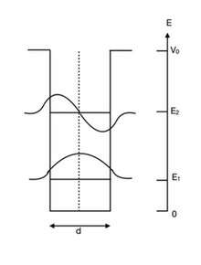
Using the relevant boundary conditions and the condition that the wave function must be continuous at the edge of the well, we get solutions for the wave vector k that satisfy the following transcendental equations:
(Even)
and
, (Odd)
where κ is the exponential decay constant in the barrier region, which is a measure of how fast the wave function decays to zero in the barrier region. The quantized energy eigenstates inside the well, which depend on the wave vector and the quantum number (n) are given by:
.
The exponential decay constant κ, is given by:
It depends on the eigenstate of a bound carrier En, the depth of the well V0, and the effective mass of the carrier within the barrier region, m*b.
The solutions to the transcendental equations above can easily be found using numerical or graphical methods. There are generally only a few solutions. However, there will always be at least one solution, so one bound state in the well, regardless of how small the potential is. Similar to the infinite well, the wave functions in the well are sinusoidal-like but exponentially decay in the barrier of the well. This has the effect of reducing the bound energy states of the quantum well compared to the infinite well.[3]
Superlattices
A superlattice is a periodic heterostructure made of alternating materials with different band-gaps. The thickness of these periodic layers is generally of the order of a few nanometers. The band structure that results from such a configuration is a period series of quantum wells. It is important that these barriers are thin enough such that carriers can tunnel through the barrier regions of the multiple wells.[2] A defining property of superlattices is that the barriers between wells are thin enough for adjacent wells to couple. Periodic structures made of repeated quantum wells that have barriers that are too thick for adjacent wave functions to couple, are called Multiple Quantum Well (MQW) structures.[3]
Since carriers can tunnel through the barrier regions between the wells, the wave functions of neighboring wells couple together through the thin barrier, therefore, the electronic states in superlattices form delocalized minibands.[3] Solutions for the allowed energy states in superlattices is similar to that for finite quantum wells with a change in the boundary conditions that arise due to the periodicity of the structures. Since the potential is periodic, the system can be mathematically described in a similar way to a one-dimensional crystal lattice.
Applications
Because of their quasi-two-dimensional nature, electrons in quantum wells have a density of states as a function of energy that has distinct steps, versus a smooth square root dependence that is found in bulk materials. Additionally, the effective mass of holes in the valence band is changed to more closely match that of electrons in the valence band. These two factors, together with the reduced amount of active material in quantum wells, leads to better performance in optical devices such as laser diodes. As a result, quantum wells are used widely in diode lasers, including red lasers for DVDs and laser pointers, infra-red lasers in fiber optic transmitters, or in blue lasers. They are also used to make HEMTs (High Electron Mobility Transistors), which are used in low-noise electronics. Quantum well infrared photodetectors are also based on quantum wells and are used for infrared imaging.
By doping either the well itself or preferably, the barrier of a quantum well with donor impurities, a two-dimensional electron gas (2DEG) may be formed. Such a structure creates the conducting channel of a HEMT and has interesting properties at low temperature. One such feature is the quantum Hall effect, seen at high magnetic fields. Acceptor dopants can also lead to a two-dimensional hole gas (2DHG).
Saturable absorber
A quantum well can be fabricated as a saturable absorber utilizing its saturable absorption property. Saturable absorbers are widely used in passively mode locking lasers. Semiconductor saturable absorbers (SESAMs) were used for laser mode-locking as early as 1974 when p-type germanium was used to mode lock a CO2 laser which generated pulses ~500 ps. Modern SESAMs are III-V semiconductor single quantum well (SQW) or multiple quantum wells (MQW) grown on semiconductor distributed Bragg reflectors (DBRs). They were initially used in a Resonant Pulse Modelocking (RPM) scheme as starting mechanisms for Ti:sapphire lasers which employed KLM as a fast saturable absorber. RPM is another coupled-cavity mode-locking technique. Different from APM lasers that employ non-resonant Kerr-type phase nonlinearity for pulse shortening, RPM employs the amplitude nonlinearity provided by the resonant band filling effects of semiconductors. SESAMs were soon developed into intracavity saturable absorber devices because of more inherent simplicity with this structure. Since then, the use of SESAMs has enabled the pulse durations, average powers, pulse energies and repetition rates of ultrafast solid-state lasers to be improved by several orders of magnitude. Average power of 60 W and repetition rate up to 160 GHz were obtained. By using SESAM-assisted KLM, sub-6 fs pulses directly from a Ti:sapphire oscillator was achieved. A major advantage SESAMs have over other saturable absorber techniques is that absorber parameters can be easily controlled over a wide range of values. For example, saturation fluence can be controlled by varying the reflectivity of the top reflector while modulation depth and recovery time can be tailored by changing the low-temperature growing conditions for the absorber layers. This freedom of design has further extended the application of SESAMs into mode-locking of fibre lasers where a relatively high modulation depth is needed to ensure self-starting and operation stability. Fibre lasers working at ~1 μm and 1.5 μm were successfully demonstrated.[7]
Thermoelectrics
Quantum wells have shown promise for energy harvesting as thermoelectric devices. They are claimed to be easier to fabricate and offer the potential to operate at room temperature. The wells connect a central cavity to two electronic reservoirs. The central cavity is kept at a hotter temperature than the reservoirs. The wells act as filters that allow electrons of certain energies to pass through. In general, greater temperature differences between the cavity and the reservoirs increases electron flow and output power.[8][9]
An experimental device delivered output power of about 0.18 W/cm2 for a temperature difference of 1 K, nearly double the power of a quantum dot energy harvester. The extra degrees of freedom allowed larger currents. Its efficiency is slightly lower than the quantum dot energy harvesters. Quantum wells transmit electrons of any energy above a certain level, while quantum dots pass only electrons of a specific energy.[8]
One possible application is to convert waste heat from electric circuits, e.g., in computer chips, back into electricity, reducing the need for cooling and energy to power the chip.[8]
Solar cells
Quantum wells have been proposed to increase the efficiency of solar cells. The theoretical maximum efficiency of traditional single-junction cells is about 34%, due in large part to their inability to capture many different wavelengths of light. Multi-junction solar cells, which consist of multiple p-n junctions of different bandgaps connected in series, increase the theoretical efficiency by broadening the range of absorbed wavelengths, but their complexity and manufacturing cost limit their use to niche applications. On the other hand, cells consisting of a p-i-n junction in which the intrinsic region contains one or more quantum wells, lead to an increased photocurrent over dark current, resulting in a net efficiency increase over conventional p-n cells.[10] Photons of energy within the well depth are absorbed in the wells and generate electron-hole pairs. In room temperature conditions, these photo-generated carriers have sufficient thermal energy to escape the well faster than the recombination rate.[11] Elaborate multi-junction quantum well solar cells can be fabricated using layer-by-layer deposition techniques such as molecular beam epitaxy or chemical vapor deposition. It has also been shown that metal or dielectric nanoparticles added above the cell lead to further increases in photo-absorption by scattering incident light into lateral propagation paths confined within the multiple-quantum-well intrinsic layer.[12]
Current study into the physics and application of quantum well solar cells
Single-junction solar cells
With conventional single-junction photovoltaic solar cells, the power it generates is the product of the photocurrent and voltage across the diode.[13] As semiconductors only absorb photons with energies higher than their bandgap, smaller bandgap material absorbs more of the sun's radiative spectrum resulting in a larger current. The highest open-circuit voltage achievable is the built-in bandgap of the material.[13] Because the bandgap of the semiconductor determines both the Current and Voltage, designing a solar cell is always a trade-off between maximizing current output with a low bandgap and voltage output with a high bandgap.[14] The maximum theoretical limit of efficiency for conventional solar cells is determined to be only 31%, with the best silicon devices achieving an optimal limit of 25%.[13]
With the introduction of quantum wells (QWs), the efficiency limit of single-junction strained QW silicon devices have increased to 28.3%.[13] The increase is due to the bandgap of the barrier material determining the built-in voltage. Whereas the bandgap of the QWs is now what determines the absorption limit.[13] With their experiments on p-i-n junction photodiodes, Barnham's group showed that placing QWs in the depleted region increases the efficiency of a device.[15] Researchers infer that the resulting increase indicates that the generation of new carriers and photocurrent due to the inclusion of lower energies in the absorption spectrum outweighs the drop in terminal voltage resulting from the recombination of carriers trapped in the quantum wells. Further studies have been able to conclude that the photocurrent increase is directly related to the redshift of the absorption spectrum.[15]
Multi-junction solar cells
Nowadays, among non-QW solar cells, the III/V multi-junction solar cells are the most efficient, recording a maximum efficiency of 46% under high sunlight concentrations. Multi-junction solar cells are created by stacking multiple p-i-n junctions of different bandgaps.[6] The efficiency of the solar cell increases with the inclusion of more of the solar radiation in the absorption spectrum by introducing more QWs of different bandgaps. The direct relation between the bandgap and lattice constant hinders the advancement of multi-junction solar cells. As more Quantum Wells(QWs) are grown together, the material grows with dislocations due to the varying lattice constants. Dislocations reduce the diffusion length and carrier lifetime.[6] Hence, QWs provide an alternate approach to multi-junction solar cells with minimal crystal dislocation.
Bandgap energy
Researchers are looking to use QWs to grow high-quality material with minimal crystal dislocations and increase the efficiency of light absorption and carrier collection to realize higher efficiency QW solar cells. Bandgap tunability helps researchers with designing their solar cells. We can estimate the effective bandgap as the function of the bandgap energy of the QW and the shift in bandgap energy due to the steric strain, Quantum Confinement Stark Effect (QCSE), and Quantum Size Effect (QSE).[6]
The strain of the material causes two effects to the bandgap energy. First is the change in relative energy of the conduction and valence band. This energy change is affected by the strain, , elastic stiffness coefficients, and , and hydrostatic deformation potential, .[6][16]
Second, due to the strain, there is a splitting of heavy-hole and light-hole degeneracy. In a heavily compressed material, the heavy-holes(hh) move to a higher energy state. In tensile material, light-holes(lh) move to a higher energy state. [6] [17] One can calculate the difference in energy due to the splitting of hh and lh from the shear deformation potential, , strain, , and elastic stiffness coefficients, and .[17]
The Quantum confinement Stark Effect induces a well-thickness dependent shift in the bandgap. Where is the elemental charge, and is the effective width of QWs in the conduction and valence band. is the induced electric field due to piezoelectric and spontaneous polarization. the reduced Planck's constant.[6]
The Quantum size effect (QSEs) can is the discretization of energy a charge carrier undergoes due to confinement when it's Bohr radius is larger than the size of the well. As the quantum well thickness increases, QSEs decrease. The decrease in QSEs causes the n=1 state to move down and decrease the effective bandgap.[6] Kronig-Penny model is used to calculate the quantum states[18], and Anderson's rule is applied to estimate the conduction band and valence band offsets in energy.[19]
Carrier capture and lifetime
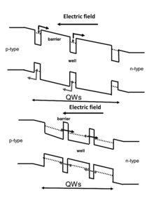
With the effective use of carriers in the QWs, researchers can increase the efficiency of Quantum Well Solar Cells(QWSCs). Within QWs in the intrinsic region of the p-i-n solar cells, optically generated carriers are either collected by the built-in field or lost due to carrier recombination. [6] Carrier recombination is the process in which a hole and electron recombine to cancel their charges. Carriers can be collected through drift by the electric field. One can either use thin wells and transport carriers via thermionic emission or use thin barriers and transport carriers via tunneling.
Carrier lifetime for escape is determined by tunneling and thermionic emission lifetimes. Tunneling and thermionic emission lifetimes both depend on having a low effective barrier height. They are expressed through the following equations[6][20]:
Where and are effective masses of charge carriers in the barrier and well, is the effective barrier height and the electric field.
Then one can calculate the escape lifetime by the following[6][20]:
The total probability of minority carriers escaping from QWs is a sum of the probability of each well,
.[20]
Where Pi is ,[20]
Where is recombination lifetime, and N is the total number of QWs in the intrinsic region.
For << , there is a high probability for carrier recollection. Assumptions made in this method of modeling are that each carrier crosses N QWs, whereas, in reality, they cross different numbers of QWs and that a carrier capture is at 100%, which may not be true in high background doping conditions.[6]
For example, taking In0.18Ga0.82As (125)/GaAs0.36P0.64 (40) into consideration, tunneling, and thermionic emission lifetimes are 0.89 and 1.84, respectively. Even if a recombination time of 50ns is assumed, the escape probability of a single quantum well and a 100 quantum wells is 0.984 and 0.1686, which is not sufficient for efficient carrier capture.[6] Reducing the barrier thickness to 20Angstroms reduces to 4.1276 ps, increasing the escape probability over a 100 QWs to 0.9918. Indicating that using thin-barriers is essential for more efficient carrier collection.[6]
Sustainability of quantum well devices compared to bulk material in light of performance
In the 1.1-1.3 eV range, Sayed et al.[6] compares the external quantum efficiency (EQE) of a metamorphic InGaAs bulk subcell on Ge substrates by Spectrolab[21] to a 100-period In0.30Ga0.70As(3.5 nm)/GaAs(2.7 nm)/ GaAs0.60P0.40(3.0 nm) QWSC by Fuji et al.[22]. The bulk material shows higher EQE values than those of QWs in the 880-900nm region, whereas the QWs have higher EQE values in the 400-600nm range.[6] This result provides some evidence that there is a struggle of extending the QWs' absorption thresholds to longer wavelengths due to strain balance and carrier transport issues. However, the bulk material has more deformations leading to low minority carrier lifetimes. [6]
In the 1.6-1.8 range, the lattice-matched AlGaAs by Heckelman et al.[23] and InGaAsP by Jain et al.[24] are compared by Sayed[6] with the lattice-matched InGaAsP/InGaP QW structure by Sayed et al.[25]. Like the 1.1-1.3eV range, the EQE of the bulk material is higher in the longer wavelength region of the spectrum, but QWs are advantageous in the sense that they absorb a broader region in the spectrum. Furthermore, hey can be grown in lower temperatures preventing thermal degradation.[6]
The application of Quantum Wells in many devices is a viable solution to increasing the energy efficiency of such devices. With lasers, the improvement has already lead to significant results like the LED. With QWSCs harvesting energy from the sun become a more potent method of cultivating energy by being able to absorb more of the sun's radiation and by being able to capture such energy from the charge carriers more efficiently. A viable option such as QWSCs provides the public with an opportunity to move away from greenhouse gas inducing methods to a greener alternative, solar energy.
See also
- Particle in a box
- Quantum wire, carriers confined in two dimensions.
- Quantum dot, carriers confined in all three dimensions.
- Quantum well laser
- Modulating retro-reflector
References
- "Quantum Well Infrared Photon Detectors | IRnova". www.ir-nova.se. Retrieved 2018-09-04.
- Odoh, E. O., & Njapba, A. S. (2015). A review of semiconductor quantum well devices. Adv. Phys. Theor. Appl, 46, 26-32.
- Fox, Mark; Ispasoiu, Radu (2006), "Quantum Wells, Superlattices, and Band-Gap Engineering", Springer Handbook of Electronic and Photonic Materials, Springer US, pp. 1021–1040, doi:10.1007/978-0-387-29185-7_42, ISBN 978-0-387-26059-4
- Nag, B. R. (2002). Physics of quantum well devices. Kluwer Academic Publishers. OCLC 754036669.
- Simon, Steven H. (2017). The Oxford solid state basics. Oxford University Press. ISBN 978-0-19-968077-1. OCLC 1091723162.
- Sayed, Islam; Bedair, S. M. (2 March 2019). "Quantum Well Solar Cells: Principles, Recent Progress, and Potential". IEEE Journal of Photovoltaics. 9 (2): 402–423. doi:10.1109/JPHOTOV.2019.2892079. ISSN 2156-3381.
- Tang, D.; Zhang, H.; Zhao, L.; Wu, X. (2008). "Observation of High-Order Polarization-Locked Vector Solitons in a Fiber Laser" (PDF). Physical Review Letters. 101 (15): 153904. arXiv:0903.2392. Bibcode:2008PhRvL.101o3904T. doi:10.1103/PhysRevLett.101.153904. PMID 18999601. Archived from the original (PDF) on January 20, 2010.
- "Scientists propose quantum wells as high-power, easy-to-make energy harvesters". Phys.org. Retrieved 2013-10-24.
- Sothmann, B. R.; Sánchez, R.; Jordan, A. N.; Büttiker, M. (2013). "Powerful energy harvester based on resonant-tunneling quantum wells". New Journal of Physics. 15 (9): 095021. arXiv:1309.7907. Bibcode:2013NJPh...15i5021S. doi:10.1088/1367-2630/15/9/095021.
- Barnham, K.; Zachariou, A. (1997). "Quantum well solar cells". Applied Surface Science. 113-114: 722–733. Bibcode:1997ApSS..113..722B. doi:10.1016/S0169-4332(96)00876-8.
- Ramey, S. M.; Khoie, R. (2003). "Modeling of multiple-quantum-well solar cells including capture, escape, and recombination of photoexcited carriers in quantum wells". IEEE Transactions on Electron Devices. 50 (5): 1179–1188. Bibcode:2003ITED...50.1179R. doi:10.1109/TED.2003.813475.
- Derkacs, D.; Chen, W. V.; Matheu, P. M.; Lim, S. H.; Yu, P. K. L.; Yu, E. T. (2008). "Nanoparticle-induced light scattering for improved performance of quantum-well solar cells". Applied Physics Letters. 93 (9): 091107. Bibcode:2008ApPhL..93i1107D. doi:10.1063/1.2973988.
- Fox, Mark; Ispasoiu, Radu (2017), Kasap, Safa; Capper, Peter (eds.), "Quantum Wells, Superlattices, and Band-Gap Engineering", Springer Handbook of Electronic and Photonic Materials, Springer International Publishing, p. 1, doi:10.1007/978-3-319-48933-9_40, ISBN 978-3-319-48931-5
- Barnham, Keith; Ballard, Ian; Barnes, Jenny; Connolly, James; Griffin, Paul; Kluftinger, Benjamin; Nelson, Jenny; Tsui, Ernest; Zachariou, Alexander (1997-04-01). "Quantum well solar cells". Applied Surface Science. Proceedings of the Eighth International Conference on Solid Films and Surfaces. 113-114: 722–733. Bibcode:1997ApSS..113..722B. doi:10.1016/S0169-4332(96)00876-8. ISSN 0169-4332.
- Anderson, Neal G. (13 April 1995). "Ideal theory of quantum well solar cells". Journal of Applied Physics. 78 (3): 1850–1861. Bibcode:1995JAP....78.1850A. doi:10.1063/1.360219. ISSN 0021-8979.
- Asai, Hiromitsu; Oe, Kunishige (1983). "Energy band‐gap shift with elastic strain in GaxIn1−xP epitaxial layers on (001) GaAs substrates". Journal of Applied Physics. 54 (4): 2052–2056. doi:10.1063/1.332252. ISSN 0021-8979.
- Adachi, Sadao (1982). "Material parameters of In1−xGaxAsyP1−yand related binaries". Journal of Applied Physics. 53 (12): 8775–8792. doi:10.1063/1.330480. ISSN 0021-8979.
- "Quantum Wires and Dots", Quantum Wells, Wires and Dots, John Wiley & Sons, Ltd, 2006-01-27, pp. 243–270, doi:10.1002/0470010827.ch8, ISBN 978-0-470-01082-2
- Anderson, R. L. (1960). "Germanium-Gallium Arsenide Heterojunctions [Letter to the Editor]". IBM Journal of Research and Development. 4 (3): 283–287. doi:10.1147/rd.43.0283. ISSN 0018-8646.
- Nelson, J.; Paxman, M.; Barnham, K.W.J.; Roberts, J.S.; Button, C. (June 1993). "Steady-state carrier escape from single quantum wells". IEEE Journal of Quantum Electronics. 29 (6): 1460–1468. Bibcode:1993IJQE...29.1460N. doi:10.1109/3.234396. ISSN 0018-9197.
- King, R., Law, D., Fetzer, C., Sherif, R., Edmondson, K., Kurtz, S., ... & Karam, N. H. (2005, June). Pathways to 40%-efficient concentrator photovoltaics. In Proc. 20th European Photovoltaic Solar Energy Conference (pp. 10-11).
- Fujii, Hiromasa; Toprasertpong, Kasidit; Wang, Yunpeng; Watanabe, Kentaroh; Sugiyama, Masakazu; Nakano, Yoshiaki (2014). "100-period, 1.23-eV bandgap InGaAs/GaAsP quantum wells for high-efficiency GaAs solar cells: Toward current-matched Ge-based tandem cells". Progress in Photovoltaics: Research and Applications. 22 (7): 784–795. doi:10.1002/pip.2454.
- Heckelmann, Stefan; Lackner, David; Karcher, Christian; Dimroth, Frank; Bett, Andreas W. (2015). "Investigations on AlxGa1-xAs Solar Cells Grown by MOVPE". IEEE Journal of Photovoltaics. 5 (1): 446–453. doi:10.1109/jphotov.2014.2367869.
- Jain, Nikhil; Geisz, John F.; France, Ryan M.; Norman, Andrew G.; Steiner, Myles A. (2017). "Enhanced Current Collection in 1.7 eV GaInAsP Solar Cells Grown on GaAs by Metalorganic Vapor Phase Epitaxy". IEEE Journal of Photovoltaics. 7 (3): 927–933. doi:10.1109/jphotov.2017.2655035.
- Sayed, Islam E. H.; Jain, Nikhil; Steiner, Myles A.; Geisz, John F.; Bedair, S. M. (2017). "100-period InGaAsP/InGaP superlattice solar cell with sub-bandgap quantum efficiency approaching 80%". Applied Physics Letters. 111 (8): 082107. Bibcode:2017ApPhL.111h2107S. doi:10.1063/1.4993888.
Further reading
- Thomas Engel, Philip Reid Quantum Chemistry and Spectroscopy. ISBN 0-8053-3843-8. Pearson Education, 2006. Pages 73–75.