Molecular electronics
Molecular electronics is the study and application of molecular building blocks for the fabrication of electronic components. It is an interdisciplinary area that spans physics, chemistry, and materials science. The unifying feature is use of molecular building blocks to fabricate electronic components. Due to the prospect of size reduction in electronics offered by molecular-level control of properties, molecular electronics has generated much excitement. It provides a potential means to extend Moore's Law beyond the foreseen limits of small-scale conventional silicon integrated circuits.[1]
Molecular scale electronics
| Part of a series of articles on |
| Nanoelectronics |
|---|
| Single-molecule electronics |
| Solid-state nanoelectronics |
| Related approaches |
|
Molecular scale electronics, also called single molecule electronics, is a branch of nanotechnology that uses single molecules, or nanoscale collections of single molecules, as electronic components. Because single molecules constitute the smallest stable structures possible, this miniaturization is the ultimate goal for shrinking electrical circuits.
Conventional electronic devices are traditionally made from bulk materials. Bulk methods have inherent limits, and are growing increasingly demanding and costly. Thus, the idea was born that the components could instead be built up atom by atom in a chemistry lab (bottom up) as opposed to carving them out of bulk material (top down). In single molecule electronics, the bulk material is replaced by single molecules. That is, instead of creating structures by removing or applying material after a pattern scaffold, the atoms are put together in a chemistry lab. The molecules used have properties that resemble traditional electronic components such as a wire, transistor, or rectifier. This concept of using a molecule as a traditional electronic component was first presented by Aviram and Ratner in 1974, when they proposed a theoretical molecular rectifier composed of donor and acceptor sites which are insulated from one another.[2]
Single molecule electronics is an emerging field, and entire electronic circuits consisting exclusively of molecular sized compounds are still very far from being realized. However, the continuous demand for more computing power, together with the inherent limits of the present day lithographic methods make the transition seem unavoidable. Currently, the focus is on discovering molecules with interesting properties and on finding ways to obtain reliable and reproducible contacts between the molecular components and the bulk material of the electrodes.
Molecular electronics operates in the quantum realm of distances less than 100 nanometers. Miniaturization down to single molecules brings the scale down to a regime where quantum mechanics effects are important. In contrast to the case in conventional electronic components, where electrons can be filled in or drawn out more or less like a continuous flow of electric charge, the transfer of a single electron alters the system significantly. The significant amount of energy due to charging has to be taken into account when making calculations about the electronic properties of the setup and is highly sensitive to distances to conducting surfaces nearby.

One of the biggest problems with measuring on single molecules is to establish reproducible electrical contact with only one molecule and doing so without shortcutting the electrodes. Because the current photolithographic technology is unable to produce electrode gaps small enough to contact both ends of the molecules tested (in the order of nanometers) alternative strategies are put into use. These include molecular-sized gaps called break junctions, in which a thin electrode is stretched until it breaks. One of the way to over come the gap size issue is by trapping molecular functionalized nanoparticles (internanoparticle spacing is match able to the size of molecules) and later target molecule by place exchange reaction.[3] Another method is to use the tip of a scanning tunneling microscope (STM) to contact molecules adhered at the other end to a metal substrate.[4] Another popular way to anchor molecules to the electrodes is to make use of sulfur's high chemical affinity to gold; though useful, the anchoring is non-specific and thus anchors the molecules randomly to all gold surfaces, and the contact resistance is highly dependent on the precise atomic geometry around the site of anchoring and thereby inherently compromises the reproducibility of the connection. To circumvent the latter issue, experiments have shown that fullerenes could be a good candidate for use instead of sulfur because of the large conjugated π-system that can electrically contact many more atoms at once than a single atom of sulfur.[5] The shift from metal electrodes to semiconductor electrodes allows for more tailored properties and thus for more interesting applications. There are some concepts for contacting organic molecules using semiconductor-only electrodes, for example by using indium arsenide nanowires with an embedded segment of the wider bandgap material indium phosphide used as an electronic barrier to be bridged by molecules.[6]
One of the biggest hindrances for single molecule electronics to be commercially exploited is the lack of means to connect a molecular sized circuit to bulk electrodes in a way that gives reproducible results. Also problematic is that some measurements on single molecules are done at cryogenic temperatures, near absolute zero, which is very energy consuming.
Molecular materials for electronics

The biggest advantage of conductive polymers is their processability, mainly by dispersion. Conductive polymers are not plastics, i.e., they are not thermoformable, yet they are organic polymers, like (insulating) polymers. They can offer high electrical conductivity but have different mechanical properties than other commercially used polymers. The electrical properties can be fine-tuned using the methods of organic synthesis[7] and of advanced dispersion.[8]
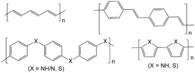
The linear-backbone polymers such as polyacetylene, polypyrrole, and polyaniline are the main classes of conductive polymers. Poly(3-alkylthiophenes) are the archetypical materials for solar cells and transistors.[7]
Conducting polymers have backbones of contiguous sp2 hybridized carbon centers. One valence electron on each center resides in a pz orbital, which is orthogonal to the other three sigma-bonds. The electrons in these delocalized orbitals have high mobility when the material is doped by oxidation, which removes some of these delocalized electrons. Thus the conjugated p-orbitals form a one-dimensional electronic band, and the electrons within this band become mobile when it is emptied partly. Despite intensive research, the relationship between morphology, chain structure, and conductivity is poorly understood yet.[9]
Due to their poor processability, conductive polymers have few large-scale applications. They have some promise in antistatic materials[7] and have been built into commercial displays and batteries, but have had limits due to the production costs, material inconsistencies, toxicity, poor solubility in solvents, and inability to directly melt process. Nevertheless, conducting polymers are rapidly gaining attraction in new uses with increasingly processable materials with better electrical and physical properties and lower costs. With the availability of stable and reproducible dispersions, poly(3,4-ethylenedioxythiophene) (PEDOT) and polyaniline have gained some large-scale applications. While PEDOT is mainly used in antistatic applications and as a transparent conductive layer in the form of PEDOT and polystyrene sulfonic acid (PSS, mixed form: PEDOT:PSS) dispersions, polyaniline is widely used to make printed circuit boards, in the final finish, to protect copper from corrosion and preventing its solderability.[8] Newer nanostructured forms of conducting polymers provide fresh impetus to this field, with their higher surface area and better dispersability.
See also
References
- Petty, M.C.; Bryce, M.R. & Bloor, D. (1995). Introduction to Molecular Electronics. New York: Oxford University Press. pp. 1–25. ISBN 0-19-521156-1.
- Aviram, Arieh; Ratner, Mark A. (15 November 1974). "Molecular rectifiers". Chemical Physics Letters. 29 (2): 277–283. Bibcode:1974CPL....29..277A. doi:10.1016/0009-2614(74)85031-1.
- Jafri, S. H. M.; et al. (2010). Nanotechnology. 21: 435204. doi:10.1088/0957-4484/21/43/435204 http://iopscience.iop.org/article/10.1088/0957-4484/21/43/435204/meta. Missing or empty
|title=(help) - Gimzewski, J.K.; Joachim, C. (1999). "Nanoscale science of single molecules using local probes". Science. 283 (5408): 1683–1688. Bibcode:1999Sci...283.1683G. doi:10.1126/science.283.5408.1683. PMID 10073926.
- Sørensen, J.K. Archived 2016-03-29 at the Wayback Machine. (2006). "Synthesis of new components, functionalized with (60)fullerene, for molecular electronics". 4th Annual meeting - CONT 2006, University of Copenhagen.
- Schukfeh, Muhammed Ihab; Storm, Kristian; Mahmoud, Ahmad; Søndergaard, Roar R.; Szwajca, Anna; Hansen, Allan; Hinze, Peter; Weimann, Thomas; Fahlvik Svensson, Sofia; Bora, Achyut; Dick, Kimberly A.; Thelander, Claes; Krebs, Frederik C.; Lugli, Paolo; Samuelson, Lars; Tornow, Marc (2013). "Conductance Enhancement of InAs/InP Heterostructure Nanowires by Surface Functionalization with Oligo(phenylene vinylene)s". ACS Nano. 7 (5): 4111–4118. doi:10.1021/nn400380g. PMID 23631558.
- Herbert Naarmann "Polymers, Electrically Conducting" in Ullmann's Encyclopedia of Industrial Chemistry 2002 Wiley-VCH, Weinheim. doi:10.1002/14356007.a21_429
- Handbook of Nanostructured Materials and Nanotechnology; Nalwa, H.S., Ed.; Academic Press: New York, NY, USA, 2000; Volume 5, pp. 501–575.
- Skotheim, T., Elsenbaumer, R., Reynolds, J., Eds.; Handbook of Conducting Polymers, 2nd ed.; Marcel Dekker, Inc.: New York, NY, USA, 1998
Further reading
- Heath, J. R. (2009). "Molecular Electronics". Annual Review of Materials Research. 39: 1–23. Bibcode:2009AnRMS..39....1H. doi:10.1146/annurev-matsci-082908-145401.
External links
