Cadmium sulfide
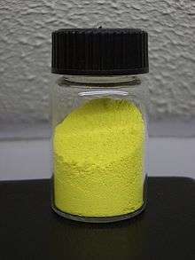
Cadmium sulfide is the inorganic compound with the formula CdS. Cadmium sulfide is a yellow solid.[4] It occurs in nature with two different crystal structures as the rare minerals greenockite and hawleyite, but is more prevalent as an impurity substituent in the similarly structured zinc ores sphalerite and wurtzite, which are the major economic sources of cadmium. As a compound that is easy to isolate and purify, it is the principal source of cadmium for all commercial applications.[4] Its vivid yellow color led to its adoption as a pigment for the yellow paint "cadmium yellow" in the 18th century.
| |||
 | |||
| Names | |||
|---|---|---|---|
| Other names | |||
| Identifiers | |||
3D model (JSmol) |
| ||
| ChEBI | |||
| ChemSpider | |||
| ECHA InfoCard | 100.013.771 | ||
| EC Number |
| ||
| 13655 | |||
PubChem CID |
|||
| RTECS number |
| ||
| UNII | |||
| UN number | 2570 | ||
CompTox Dashboard (EPA) |
|||
| |||
| |||
| Properties | |||
| CdS | |||
| Molar mass | 144.47 g·mol−1 | ||
| Appearance | Yellow-orange to brown solid. | ||
| Density | 4.826 g/cm3, solid. | ||
| Melting point | 1,750 °C (3,180 °F; 2,020 K) 10 MPa | ||
| Boiling point | 980 °C (1,800 °F; 1,250 K) (sublimation) | ||
| insoluble[1] | |||
| Solubility | soluble in acid very slightly soluble in ammonium hydroxide | ||
| -50.0·10−6 cm3/mol | |||
Refractive index (nD) |
2.529 | ||
| Structure | |||
| Hexagonal, Cubic | |||
| Thermochemistry | |||
Std molar entropy (S |
65 J·mol−1·K−1[2] | ||
Std enthalpy of formation (ΔfH⦵298) |
−162 kJ·mol−1[2] | ||
| Hazards | |||
| Safety data sheet | ICSC 0404 | ||
| GHS pictograms |   | ||
| GHS Signal word | Danger | ||
GHS hazard statements |
H302, H341, H350, H361, H372, H413 | ||
| P201, P202, P260, P264, P270, P273, P281, P301+312, P308+313, P314, P330, P405, P501 | |||
| NFPA 704 (fire diamond) | |||
| Flash point | Non-flammable | ||
| Lethal dose or concentration (LD, LC): | |||
LD50 (median dose) |
7080 mg/kg (rat, oral) | ||
| NIOSH (US health exposure limits): | |||
PEL (Permissible) |
[1910.1027] TWA 0.005 mg/m3 (as Cd)[3] | ||
REL (Recommended) |
Ca[3] | ||
IDLH (Immediate danger) |
Ca [9 mg/m3 (as Cd)][3] | ||
| Related compounds | |||
Other anions |
Cadmium oxide Cadmium selenide | ||
Other cations |
Zinc sulfide Mercury sulfide | ||
Except where otherwise noted, data are given for materials in their standard state (at 25 °C [77 °F], 100 kPa). | |||
| Infobox references | |||
Production
Cadmium sulfide can be prepared by the precipitation from soluble cadmium(II) salts with sulfide ion. This reaction has been used for gravimetric analysis and qualitative inorganic analysis.[5]
The preparative route and the subsequent treatment of the product, affects the polymorphic form that is produced (i.e., cubic vs hexagonal). It has been asserted that chemical precipitation methods result in the cubic zincblende form.[6]
Pigment production usually involves the precipitation of CdS, the washing of the solid precipitate to remove soluble cadmium salts followed by calcination (roasting) to convert it to the hexagonal form followed by milling to produce a powder.[7] When cadmium sulfide selenides are required the CdSe is co-precipitated with CdS and the cadmium sulfoselenide is created during the calcination step.[7]
Cadmium sulfide is sometimes associated with sulfate reducing bacteria.[8][9]
Routes to thin films of CdS
Special methods are used to produce films of CdS as components in some photoresistors and solar cells. In the chemical bath deposition method, thin films of CdS have been prepared using thiourea as the source of sulfide anions and an ammonium buffer solution to control pH:[10]
- Cd2+ + H2O + (NH2)2CS + 2 NH3 → CdS + (NH2)2CO + 2 NH4+
Cadmium sulfide can be produced using metalorganic vapour phase epitaxy and MOCVD techniques by the reaction of dimethylcadmium with diethyl sulfide:[11]
- Cd(CH3)2 + Et2S → CdS + CH3CH3 + C4H10
Other methods to produce films of CdS include
- Sol gel techniques[12]
- Sputtering[13]
- Electrochemical deposition[14]
- Spraying with precursor cadmium salt, sulfur compound and dopant[15]
- Screen printing using a slurry containing dispersed CdS[16]
Reactions
Cadmium sulfide can be dissolved in acids.[17]
- CdS + 2 HCl → CdCl2 + H2S
When solutions of sulfide containing dispersed CdS particles are irradiated with light hydrogen gas is generated:[18]
- H2S → H2 + S ΔHf = +9.4 kcal/mol
The proposed mechanism involves the electron/hole pairs created when incident light is absorbed by the cadmium sulfide[19] followed by these reacting with water and sulfide:[18]
- Production of an electron hole pair
- CdS + hν → e− + hole+
- Reaction of electron
- 2e− + 2H2O → H2 + 2OH−
- Reaction of hole
- 2hole+ + S2− → S
Structure and physical properties
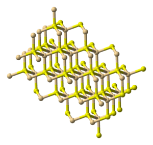
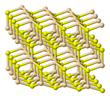
Cadmium sulfide has, like zinc sulfide, two crystal forms. The more stable hexagonal wurtzite structure (found in the mineral Greenockite) and the cubic zinc blende structure (found in the mineral Hawleyite). In both of these forms the cadmium and sulfur atoms are four coordinate.[20] There is also a high pressure form with the NaCl rock salt structure.[20]
Cadmium sulfide is a direct band gap semiconductor (gap 2.42 eV[19]). The proximity of its band gap to visible light wavelengths gives it a coloured appearance.[4]
As well as this obvious property other properties result:
- the conductivity increases when irradiated,[19] (leading to uses as a photoresistor)
- when combined with a p-type semiconductor it forms the core component of a photovoltaic (solar) cell and a CdS/Cu2S solar cell was one of the first efficient cells to be reported (1954)[21][22]
- when doped with for example Cu+ ("activator") and Al3+ ("coactivator") CdS luminesces under electron beam excitation (cathodoluminescence) and is used as phosphor[23]
- both polymorphs are piezoelectric and the hexagonal is also pyroelectric[24]
- electroluminescence[25]
- CdS crystal can act as a solid state laser[26][27]
- In thin-film form, CdS can be combined with other layers for use in certain types of solar cells.[28] CdS was also one of the first semiconductor materials to be used for thin-film transistors (TFTs).[29] However interest in compound semiconductors for TFTs largely waned after the emergence of amorphous silicon technology in the late 1970s.
- Thin films of CdS can be piezoelectric and have been used as transducers which can operate at frequencies in the GHz region.
- Nanoribbons of CdS show a net cooling due annihilation of phonons, during anti-Stokes luminescence at ~510 nm. As a result, a maximum temperature drop of 40 and 15 K has been demonstrated when the nanoribbons are pumped with a 514 or 532 nm laser.[30]
Applications
Pigment
CdS is used as pigment in plastics, showing good thermal stability, light and weather fastness, chemical resistance and high opacity.[7] As a pigment, CdS is known as cadmium yellow.[4] (CI pigment yellow 37[31]) About 2000 tons are produced annually as of 1982, representing about 25% of the cadmium processed commercially.[32]
Historical use in art
The general commercial availability of cadmium sulfide from the 1840s led to its adoption by artists, notably Van Gogh, Monet (in his London series and other works) and Matisse (Bathers by a river 1916–1919).[33] The presence of cadmium in paints has been used to detect forgeries in paintings alleged to have been produced prior to the 19th century.[34]
CdS-CdSe solutions
CdS and CdSe form solid solutions. Increasing amounts of cadmium selenide, gives pigments verging toward red, for example CI pigment orange 20 and CI pigment red 108.[31]
Such solid solutions are components of photoresistors (light dependent resistors) sensitive to visible and near infrared light.
Safety
Cadmium sulfide is toxic, especially dangerous when inhaled as dust, and cadmium compounds general are classified as carcinogenic.[35] Problems of biocompatibility have been reported when CdS is used as colors in tattoos.[36]
References
- Lide, David R. (1998). Handbook of Chemistry and Physics (87 ed.). Boca Raton, FL: CRC Press. pp. 4–67, 1363. ISBN 978-0-8493-0594-8.
- Zumdahl, Steven S. (2009). Chemical Principles 6th Ed. Houghton Mifflin Company. p. A21. ISBN 978-0-618-94690-7.
- NIOSH Pocket Guide to Chemical Hazards. "#0087". National Institute for Occupational Safety and Health (NIOSH).
- Egon Wiberg, Arnold Frederick Holleman (2001) Inorganic Chemistry, Elsevier ISBN 0-12-352651-5
- Fred Ibbotson (2007), The Chemical Analysis of Steel-Works' Materials,Read Books, ISBN 1-4067-8113-4
- Paul Klocek (1991), Handbook of Infrared Optical Materials, CRC Press ISBN 0-8247-8468-5
- Hugh MacDonald Smith (2002). High Performance Pigments. Wiley-VCH. ISBN 978-3-527-30204-8.
- Larry L. Barton 1995 Sulfate reducing bacteria, Springer, ISBN 0-306-44857-2
- Sweeney, Rozamond Y.; Mao, Chuanbin; Gao, Xiaoxia; Burt, Justin L.; Belcher, Angela M.; Georgiou, George; Iverson, Brent L. (2004). "Bacterial Biosynthesis of Cadmium Sulfide Nanocrystals". Chemistry & Biology. 11 (11): 1553–9. doi:10.1016/j.chembiol.2004.08.022. PMID 15556006.
- Oladeji, I.O.; Chow, L. (1997). "Optimization of Chemical Bath Deposited Cadmium Sulfide". J. Electrochem. Soc. 144 (7): 7. CiteSeerX 10.1.1.563.1643. doi:10.1149/1.1837815.
- Uda, H; Yonezawa, H; Ohtsubo, Y; Kosaka, M; Sonomura, H (2003). "Thin CdS films prepared by metalorganic chemical vapor deposition". Solar Energy Materials and Solar Cells. 75 (1–2): 219. doi:10.1016/S0927-0248(02)00163-0.
- Reisfeld, R (2002). "Nanosized semiconductor particles in glasses prepared by the sol–gel method: their optical properties and potential uses". Journal of Alloys and Compounds. 341 (1–2): 56. doi:10.1016/S0925-8388(02)00059-2.
- Moon, B; Lee, J; Jung, H (2006). "Comparative studies of the properties of CdS films deposited on different substrates by R.F. sputtering". Thin Solid Films. 511–512: 299. Bibcode:2006TSF...511..299M. doi:10.1016/j.tsf.2005.11.080.
- Goto, F; Shirai, Katsunori; Ichimura, Masaya (1998). "Defect reduction in electrochemically deposited CdS thin films by annealing in O2". Solar Energy Materials and Solar Cells. 50 (1–4): 147. doi:10.1016/S0927-0248(97)00136-0.
- U.S. Patent 4,086,101 Photovoltaic cells, J.F. Jordan, C.M. Lampkin Issue date: April 25, 1978
- U.S. Patent 3,208,022, High performance photoresistor, Y.T. Sihvonen, issue date: September 21, 1965
- Wanrooij, P. H. P.; Agarwal, U. S.; Meuldijk, J.; Kasteren, J. M. N. van; Lemstra, P. J. (2006). "Extraction of CdS pigment from waste polyethylene". Journal of Applied Polymer Science. 100 (2): 1024. doi:10.1002/app.22962.
- Mario Schiavello (1985) Photoelectrochemistry, Photocatalysis, and Photoreactors: Fundamentals and Developments Springer ISBN 90-277-1946-2
- D. Lincot, Gary Hodes Chemical Solution Deposition of Semiconducting and Non-Metallic Films: Proceedings of the International Symposium The Electrochemical Society, 2006 ISBN 1-56677-433-0
- Wells A.F. (1984) Structural Inorganic Chemistry 5th edition Oxford Science Publications ISBN 0-19-855370-6
- Antonio Luque, Steven Hegedus, (2003), Handbook of Photovoltaic Science and Engineering John Wiley and Sons ISBN 0-471-49196-9
- Reynolds, D.; Leies, G.; Antes, L.; Marburger, R. (1954). "Photovoltaic Effect in Cadmium Sulfide". Physical Review. 96 (2): 533. Bibcode:1954PhRv...96..533R. doi:10.1103/PhysRev.96.533.
- C. Fouassier,(1994), Luminescence in Encyclopedia of Inorganic Chemistry, John Wiley & Sons ISBN 0-471-93620-0
- Minkus, Wilfred (1965). "Temperature Dependence of the Pyroelectric Effect in Cadmium Sulfide". Physical Review. 138 (4A): A1277–A1287. Bibcode:1965PhRv..138.1277M. doi:10.1103/PhysRev.138.A1277.
- Smith, Roland (1957). "Low-Field Electroluminescence in Insulating Crystals of Cadmium Sulfide". Physical Review. 105 (3): 900. Bibcode:1957PhRv..105..900S. doi:10.1103/PhysRev.105.900.
- Akimov, Yu A; Burov, A A; Drozhbin, Yu A; Kovalenko, V A; Kozlov, S E; Kryukova, I V; Rodichenko, G V; Stepanov, B M; Yakovlev, V A (1972). "KGP-2: An Electron-Beam-Pumped Cadmium Sulfide Laser". Soviet Journal of Quantum Electronics. 2 (3): 284. Bibcode:1972QuEle...2..284A. doi:10.1070/QE1972v002n03ABEH004443.
- Agarwal, Ritesh; Barrelet, Carl J.; Lieber, Charles M. (2005). "Lasing in Single Cadmium Sulfide Nanowire Optical Cavities". Nano Letters. 5 (5): 917–920. arXiv:cond-mat/0412144v1. Bibcode:2005NanoL...5..917A. doi:10.1021/nl050440u. PMID 15884894.
- Zhao, H.; Farah, Alvi; Morel, D.; Ferekides, C.S. (2009). "The effect of impurities on the doping and VOC of Cd Te/CDS thin film solar cells". Thin Solid Films. 517 (7): 2365–2369. Bibcode:2009TSF...517.2365Z. doi:10.1016/j.tsf.2008.11.041.
- Weimer, Paul (1962). "The TFT A New Thin-Film Transistor". Proceedings of the IRE. 50: 1462–1469. doi:10.1109/JRPROC.1962.288190.
- Zhang, Jun (24 January 2013). "Laser cooling of a semiconductor by 40 kelvin". Nature. 493 (7433): 504–508. Bibcode:2013Natur.493..504Z. doi:10.1038/nature11721. PMID 23344360.
- R. M. Christie 2001 Colour Chemistry, p. 155 Royal Society of Chemistry ISBN 0-85404-573-2
- Karl-Heinz Schulte-Schrepping, Magnus Piscator "Cadmium and Cadmium Compounds" in Ullmann's Encyclopedia of Industrial Chemistry, 2007 Wiley-VCH, Weinheim. doi:10.1002/14356007.a04_499.
- Sidney Perkowitz, 1998, Empire of Light: A History of Discovery in Science and Art Joseph Henry Press, ISBN 0-309-06556-9
- W. Stanley Taft, James W. Mayer, Richard Newman, Peter Kuniholm, Dusan Stulik (2000) The Science of Paintings, Springer, ISBN 0-387-98722-3
- CDC International Chemical Safety Card - Cadmium Sulfide ARCHIVE COPY
- Bjornberg, A (Sep 1963). "Reactions to light in yellow tattoos from cadmium sulfide". Arch Dermatol. 88 (3): 267–71. doi:10.1001/archderm.1963.01590210025003. PMID 14043617.
External links
| Wikimedia Commons has media related to Cadmium sulfide. |
- Cadmium(II) sulphide information at Webelements
- IARC Monograph: "Cadmium and Cadmium Compounds" Last access November 2005.
- International Chemical Safety Card 0404
- National Pollutant Inventory - Cadmium and compounds
- Report by the Academy of Medical Sciences to the Chief Scientific Adviser, Ministry of Defence on the zinc cadmium sulphide dispersion trials undertaken in the United Kingdom between 1953 and 1964.


