Signal integrity
Signal integrity or SI is a set of measures of the quality of an electrical signal. In digital electronics, a stream of binary values is represented by a voltage (or current) waveform. However, digital signals are fundamentally analog in nature, and all signals are subject to effects such as noise, distortion, and loss. Over short distances and at low bit rates, a simple conductor can transmit this with sufficient fidelity. At high bit rates and over longer distances or through various mediums, various effects can degrade the electrical signal to the point where errors occur and the system or device fails. Signal integrity engineering is the task of analyzing and mitigating these effects. It is an important activity at all levels of electronics packaging and assembly, from internal connections of an integrated circuit (IC),[1] through the package, the printed circuit board (PCB), the backplane, and inter-system connections.[2] While there are some common themes at these various levels, there are also practical considerations, in particular the interconnect flight time versus the bit period, that cause substantial differences in the approach to signal integrity for on-chip connections versus chip-to-chip connections.

Some of the main issues of concern for signal integrity are ringing, crosstalk, ground bounce, distortion, signal loss, and power supply noise.
History
Signal integrity primarily involves the electrical performance of the wires and other packaging structures used to move signals about within an electronic product. Such performance is a matter of basic physics and as such has remained relatively unchanged since the inception of electronic signaling. The first transatlantic telegraph cable suffered from severe signal integrity problems, and analysis of the problems yielded many of the mathematical tools still used today to analyze signal integrity problems, such as the telegrapher's equations. Products as old as the Western Electric crossbar telephone exchange (circa 1940), based on the wire-spring relay, suffered almost all the effects seen today - the ringing, crosstalk, ground bounce, and power supply noise that plague modern digital products.
On printed circuit boards, signal integrity became a serious concern when the transition (rise and fall) times of signals started to become comparable to the propagation time across the board. Very roughly speaking, this typically happens when system speeds exceed a few tens of MHz. At first, only a few of the most important, or highest speed, signals needed detailed analysis or design. As speeds increased, a larger and larger fraction of signals needed SI analysis and design practices. In modern (> 100 MHz) circuit designs, essentially all signals must be designed with SI in mind.
For ICs, SI analysis became necessary as an effect of reduced design rules. In the early days of the modern VLSI era, digital chip circuit design and layout were manual processes. The use of abstraction and the application of automatic synthesis techniques have since allowed designers to express their designs using high-level languages and apply an automated design process to create very complex designs, ignoring the electrical characteristics of the underlying circuits to a large degree. However, scaling trends (see Moore's law) brought electrical effects back to the forefront in recent technology nodes. With scaling of technology below 0.25 µm, the wire delays have become comparable or even greater than the gate delays. As a result, the wire delays needed to be considered to achieve timing closure. In nanometer technologies at 0.13 µm and below, unintended interactions between signals (e.g. crosstalk) became an important consideration for digital design. At these technology nodes, the performance and correctness of a design cannot be assured without considering noise effects.
Most of this article is about SI in relation to modern electronic technology - notably the use integrated circuits and printed circuit board technology. Nevertheless, the principles of SI are not exclusive to the signalling technology used. SI existed long before the advent of either technology, and will do so as long as electronic communications persist.
On-chip signal integrity
Signal integrity problems in modern integrated circuits (ICs) can have many drastic consequences for digital designs:
- Products can fail to operate at all, or worse yet, become unreliable in the field.
- The design may work, but only at speeds slower than planned
- Yield may be lowered, sometimes drastically
The cost of these failures is very high, and includes photomask costs, engineering costs and opportunity cost due to delayed product introduction. Therefore, electronic design automation (EDA) tools have been developed to analyze, prevent, and correct these problems.[1] In integrated circuits, or ICs, the main cause of signal integrity problems is crosstalk. In CMOS technologies, this is primarily due to coupling capacitance, but in general it may be caused by mutual inductance, substrate coupling, non-ideal gate operation, and other sources. The fixes normally involve changing the sizes of drivers and/or spacing of wires.
In analog circuits, designers are also concerned with noise that arise from physical sources, such as thermal noise, flicker noise, and shot noise. These noise sources on the one hand present a lower limit to the smallest signal that can be amplified, and on the other, define an upper limit to the useful amplification.
In digital ICs, noise in a signal of interest arises primarily from coupling effects from switching of other signals. Increasing interconnect density has led to each wire having neighbors that are physically closer together, leading to increased crosstalk between neighboring nets. As circuits have continued to shrink in accordance with Moore's law, several effects have conspired to make noise problems worse:
- To keep resistance tolerable despite decreased width, modern wire geometries are thicker in proportion to their spacing. This increases the sidewall capacitance at the expense of capacitance to ground, hence increasing the induced noise voltage (expressed as a fraction of supply voltage).
- Technology scaling has led to lower threshold voltages for MOS transistors, and has also reduced the difference between threshold and supply voltages, thereby reducing noise margins.
- Logic speeds, and clock speeds in particular, have increased significantly, thus leading to faster transition (rise and fall) times. These faster transition times are closely linked to higher capacitive crosstalk. Also, at such high speeds the inductive properties of the wires come into play, especially mutual inductance.
These effects have increased the interactions between signals and decreased the noise immunity of digital CMOS circuits. This has led to noise being a significant problem for digital ICs that must be considered by every digital chip designer prior to tape-out. There are several concerns that must be mitigated:
- Noise may cause a signal to assume the wrong value. This is particularly critical when the signal is about to be latched (or sampled), for a wrong value could be loaded into a storage element, causing logic failure.
- Noise may delay the settling of the signal to the correct value. This is often called noise-on-delay.
- Noise (e.g. ringing) may cause the input voltage of a gate to drop below ground level, or to exceed the supply voltage. This can reduce the lifetime of the device by stressing components, induce latchup, or cause multiple cycling of signals that should only cycle once in a given period.
Finding IC signal integrity problems
Typically, an IC designer would take the following steps for SI verification:
- Perform a layout extraction to get the parasitics associated with the layout. Usually worst-case parasitics and best-case parasitics are extracted and used in the simulations. For ICs, unlike PCBs, physical measurement of the parasitics is almost never done, since in-situ measurements with external equipment are extremely difficult. Furthermore, any measurement would occur after the chip has been created, which is too late to fix any problems observed.
- Create a list of expected noise events, including different types of noise, such as coupling and charge sharing.
- Create a model for each noise event. It is critical that the model is as accurate as necessary to model the given noise event.
- For each signal event, decide how to excite the circuit so that the noise event will occur.
- Create a SPICE (or another circuit simulator) netlist that represents the desired excitation, to include as many effects (such as parasitic inductance and capacitance, and various distortion effects) as necessary.
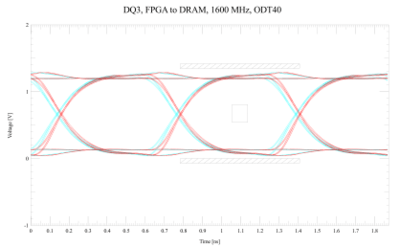
- Run SPICE simulations. Analyze the simulation results and decide whether any re-design is required. It is common to analyze the results with an eye pattern and by calculating a timing budget.[3]
Modern signal integrity tools for IC design perform all these steps automatically, producing reports that give a design a clean bill of health, or a list of problems that must be fixed. However, such tools generally are not applied across an entire IC, but only selected signals of interest.
Fixing IC signal integrity problems
Once a problem is found, it must be fixed. Typical fixes for IC on-chip problems include:
- Removing impedance discontinuities. Finding places where significant shifts in the impedance exist and adjusting the geometry of the path to shift the impedance to better match the rest of the path.
- Driver optimization. You can have too much drive, and also not enough.
- Buffer insertion. In this approach, instead of upsizing the victim driver, a buffer is inserted at an appropriate point in the victim net.
- Aggressor downsizing. This works by increasing the transition time of the attacking net by reducing the strength of its driver.
- Add shielding. Add shielding of critical nets or clock nets using GND and VDD shields to reduce the effect of crosstalk (this technique may lead to routing overhead).
- Routing changes. Routing changes can be very effective in fixing noise problems, mainly by reducing the most troublesome coupling effects via separation.
Each of these fixes may possibly cause other problems. This type of issue must be addressed as part of design flows and design closure. Re-analysis after design changes is a prudent measure.
On-die termination
On-die termination (ODT) or Digitally Controlled Impedance (DCI[4]) is the technology where the termination resistor for impedance matching in transmission lines is located within a semiconductor chip, instead of a separate, discrete device mounted on a circuit board. The closeness of the termination from the receiver shorten the stub between the two, thus improving the overall signal integrity.
Chip-to-chip signal integrity

For wired connections, it is important to compare the interconnect flight time to the bit period to decide whether an impedance matched or unmatched connection is needed.
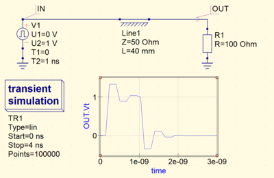
The channel flight time (delay) of the interconnect is roughly 1 ns per 15 cm (6 in) of FR-4 stripline (the propagation velocity depends on the dielectric and the geometry)[5]. Reflections of previous pulses at impedance mismatches die down after a few bounces up and down the line (i.e. on the order of the flight time). At low bit rates, the echoes die down on their own, and by midpulse, they are not a concern. Impedance matching is neither necessary nor desirable. There are many circuit board types other than FR-4, but usually they are more costly to manufacture.
The gentle trend to higher bit rates accelerated dramatically in 2004, with the introduction by Intel of the PCI-Express standard. Following this lead, the majority of chip-to-chip connection standards underwent an architectural shift from parallel buses to serializer/deserializer (SERDES) links called "lanes." Such serial links eliminate parallel bus clock skew and reduce the number of traces and resultant coupling effects but these advantages come at the cost of a large increase in bit rate on the lanes, and shorter bit periods.
At multigigabit/s data rates, link designers must consider reflections at impedance changes (e.g. where traces change levels at vias, see Transmission lines), noise induced by densely packed neighboring connections (crosstalk), and high-frequency attenuation caused by the skin effect in the metal trace and dielectric loss tangent. Examples of mitigation techniques for these impairments are a redesign of the via geometry to ensure an impedance match, use of differential signaling, and preemphasis filtering, respectively.[6][7]
At these new multigigabit/s bit rates, the bit period is shorter than the flight time; echoes of previous pulses can arrive at the receiver on top of the main pulse and corrupt it. In communication engineering this is called intersymbol interference (ISI). In signal integrity engineering it is usually called eye closure (a reference to the clutter in the center of a type of oscilloscope trace called an eye diagram). When the bit period is shorter than the flight time, elimination of reflections using classic microwave techniques like matching the electrical impedance of the transmitter to the interconnect, the sections of interconnect to each other, and the interconnect to the receiver, is crucial. Termination with a source or load is a synonym for matching at the two ends. The interconnect impedance that can be selected is constrained by the impedance of free space (~377 Ω), a geometric form factor and by the square root of the relative dielectric constant of the stripline filler (typically FR-4, with a relative dielectric constant of ~4). Together, these properties determine the trace's characteristic impedance. 50 Ω is a convenient choice for single-end lines,[8] and 100 ohm for differential.
As a consequence of the low impedance required by matching, PCB signal traces carry much more current than their on-chip counterparts. This larger current induces crosstalk primarily in a magnetic or inductive mode as opposed to a capacitive mode. To combat this crosstalk, digital PCB designers must remain acutely aware of not only the intended signal path for every signal, but also the path of returning signal current for every signal. The signal itself and its returning signal current path are equally capable of generating inductive crosstalk. Differential trace pairs help to reduce these effects.
A third difference between on-chip and chip-to-chip connection involves the cross-sectional size of the signal conductor, namely that PCB conductors are much larger (typically 100 µm or more in width). Thus, PCB traces have a small series resistance (typically 0.1 Ω/cm) at DC. The high frequency component of the pulse is however attenuated by additional resistance due to the skin effect and dielectric loss tangent associated with the PCB material.
The main challenge often depends on whether the project is a cost-driven consumer application or a performance-driven infrastructure application.[9] They tend to require extensive post-layout verification (using an EM simulator) and pre-layout design optimization (using SPICE and a channel simulator), respectively.
Routing topology


The noise levels on a trace/network is highly dependent on the routing topology selected. In a point-to-point topology, the signal is routed from the transmitter directly to the receiver (this is applied in PCIe, RapidIO, GbE, DDR2/DDR3/DDR4 DQ/DQS etc.). A point-to-point topology has the least SI-problems since there is no large impedance matches being introduced by line T's (a two-way split of a trace).
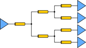
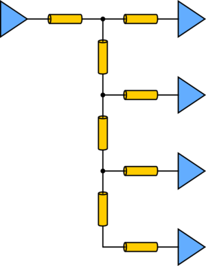
For interfaces where multiple packages are receiving from the same line, (for example with a backplane configuration), the line must be split at some point to service all receivers. Some stubs and impedance mismatches are deemed to occur. Multipackage interfaces include BLVDS, DDR2/DDR3/DDR4 C/A bank, RS485 and CAN Bus. There are two main multipackage topologies: Tree and fly-by.
Finding signal integrity problems
- Perform a layout extraction to get the parasitics associated with the layout. Usually worst-case parasitics and best-case parasitics are extracted and used in the simulations. Because of the distributed nature of many of the impairments, electromagnetic simulation[10] is used for extraction.
- If the PCB or package already exists, the designer can also measure the impairment presented by the connection using high speed instrumentation such as a vector network analyzer. For example, IEEE P802.3ap Task Force uses measured S-parameters as test cases[11] for proposed solutions to the problem of 10 Gbit/s Ethernet over backplanes.
- Accurate noise modeling is a must. Create a list of expected noise events, including different types of noise, such as coupling and charge sharing. Input Output Buffer Information Specification (IBIS) or circuit models may be used to represent drivers and receivers.
- For each noise event, decide how to excite the circuit so that the noise event will occur.
- Create a SPICE (or another circuit simulator) netlist that represents the desired excitation.
- Run SPICE and record the results.
- Analyze the simulation results and decide whether any re-design is required. To analyze the results quite often a data eye is generated and a timing budget is calculated. An example video for generating a data eye can be found on YouTube: An Eye is Born.
There are special purpose EDA tools[12] that help the engineer perform all these steps on each signal in a design, pointing out problems or verifying the design is ready for manufacture. In selecting which tool is best for a particular task, one must consider characteristics of each such as capacity (how many nodes or elements), performance (simulation speed), accuracy (how good are the models), convergence (how good is the solver), capability (non-linear versus linear, frequency dependent versus frequency independent etc.), and ease of use.
Fixing signal integrity problems
An IC package or PCB designer removes signal integrity problems through these techniques:
- Placing a solid reference plane adjacent to the signal traces to control crosstalk
- Controlling the trace width spacing to the reference plane to create consistent trace impedance
- Using terminations to control ringing
- Route traces perpendicular on adjacent layers to reduce crosstalk
- Increasing spacing between traces to reduce crosstalk
- Providing sufficient ground (and power) connections to limit ground bounce (this subdiscipline of signal integrity is sometimes called out separately as power integrity)
- Distributing power with solid plane layers to limit power supply noise
- Adding a preemphasis filter to the transmitter driving cell[13]
- Adding an equalizer to the receiving cell[13]
- Improved clock and data recovery (CDR) circuitry with low jitter/phase noise[14]
Each of these fixes may possibly cause other problems. This type of issue must be addressed as part of design flows and design closure.
Notes
- Louis Kossuth Scheffer; Luciano Lavagno; Grant Martin (eds) (2006). Electronic design automation for integrated circuits handbook. Boca Raton, Florida: CRC/Taylor & Francis. ISBN 0-8493-3096-3.CS1 maint: multiple names: authors list (link) CS1 maint: extra text: authors list (link) A survey of the field of electronic design automation. Portions of IC section of this article were derived (with permission) from Vol II, Chapter 21, Noise Considerations in Digital ICs, by Vinod Kariat.
- Howard W. Johnson; Martin Graham (1993). High speed digital design a handbook of black magic. Englewood Cliffs, New Jersey: Prentice Hall PTR. ISBN 0-13-395724-1. A book for digital PCB designers, highlighting and explaining analog circuit principles relevant to high-speed digital design.
- Ruckerbauer, Hermann. "An Eye is Born". Gives an example video of construction of an eye pattern
- Banas, David. "Using Digitally Controlled Impedance: Signal Integrity vs. Power Dissipation Considerations, XAPP863 (v1.0)" (PDF).
- "Rule of Thumb #3 Signal speed on an interconnect". EDN. Retrieved 2018-03-17.
- "Signal Integrity: Problems and Solutions," Eric Bogatin, Bogatin Enterprises
- "Eight Hints for Debugging and Validating High-Speed Buses," Application Note 1382-10, Agilent Technologies
- "Why 50 Ohms?". Microwaves101. Retrieved 2008-06-02.
- Rako, Paul (April 23, 2009). "Voices: Signal-integrity experts speak out: Two experts discuss signal-integrity challenges and their expectations for signal integrity". EDN.
For cost-driven consumer applications ... [i]t's tempting to compact [the parallel buses], but the risk is postlayout failure ... For performance-driven applications, the pinch points [is] prelayout design-space exploration ...
- "Hurdle the multigigabit per second barrier"
- IEEE P802.3ap Task Force Channel Models
- Breed, Gary (August 2008). "High Speed Digital Design Benefits from Recent EDA Tools Development" (PDF). High Frequency Electronics. p. 52. Retrieved May 1, 2009.
...with continued increase in clock rates of digital circuits, the realms of RF and digital circuits are now more closely tied than ever before.
- "Using Pre-Emphasis and Equalization with Stratix GX" (PDF). Altera.
- "Using Clock Jitter Analysis to Reduce BER in Serial Data Applications", Application Note, literature number 5989-5718EN, Agilent Technologies
References
- Howard Johnson; Martin Graham. (2002). High-speed signal propagation : advanced black magic. Upper Saddle River, New Jersey: Prentice Hall PTR. ISBN 0-13-084408-X. Advanced-level reference text for experienced digital designers who want to press their designs to the upper limits of speed and distance.
- Eric Bogatin. (2009). Signal and Power Integrity - Simplified, Second Edition. Upper Saddle River, New Jersey: Prentice Hall. ISBN 978-0-13-234979-6. Archived from the original on 2011-09-10. From the backcover: Draws from author's industrial experience and his work teaching more than five thousand engineers.
- Stephen H. Hall; Garrett W. Hall; James A. McCall. (2000). High speed digital system design : a handbook of interconnect theory and design practices. New York: Wiley. ISBN 0-471-36090-2.
- William J. Dally; John W. Poulton. (1999). Digital systems engineering. Cambridge: Cambridge Univ. Press. ISBN 0-521-59292-5. Textbook on the problems of building digital systems, including signal integrity.
- Douglas Brooks. (2003). Signal integrity issues and printed circuit board design. Upper Saddle River, New Jersey: Prentice Hall PTR. ISBN 0-13-141884-X. This book approaches electrical engineering and signal integrity principles from a basic level, assuming little prior understanding.
- Geoff Lawday; David Ireland & Greg Edlund. (2008). A signal integrity engineer's companion : real-time test and measurement and design simulation. Upper Saddle River, New Jersey: Prentice Hall. ISBN 0-13-186006-2.
- Raj; A. Ege Engin. (2008). Power integrity modeling and design for semiconductors and systems. Upper Saddle River, New Jersey: Prentice Hall. ISBN 978-0-13-615206-4. Using realistic case studies and downloadable software examples, two leading experts demonstrate today's best techniques for designing and modeling interconnects to efficiently distribute power and minimize noise. The authors carefully introduce the core concepts of power distribution design, systematically present and compare leading techniques for modeling noise, and link these techniques to specific applications. Their many examples range from the simplest (using analytical equations to compute power supply noise) through complex system-level applications.
- Signal Integrity for PCB Designers
- Altera Signal Integrity Center
- Basic Principles of Signal Integrity
- Agilent EEsof EDA - Signal Integrity Analysis Resources
- "Design tip: Model instruments to improve signal integrity simulation", EETimes, John Olah, 2007-October-25
- Topics in signal integrity were discussed at DesignCon 2008 February 4, 2008 to February 7, 2008
- "Understanding Signal Integrity - Signal integrity is becoming a more significant problem as clock frequencies increase" by Eric Bogatin, GigaTest Labs, Agilent Application Note 5988-5978EN, April 2002, 8 pages, PDF, 0.9MB
- "Signal Integrity Analysis Series Part 1: Single-Port TDR, TDR/TDT, and 2-Port TDR" (Agilent Application Note 5989-5763EN, February 2007, 72 pages, PDF, 5.2MB)
- "Signal Integrity Analysis Series Part 2: 4-Port TDR/VNA/PLTS" (Agilent Application Note 5989-5764EN, February 2007, 56 pages, PDF, 3.6MB)
- "Signal Integrity Analysis Series Part 3: The ABC's of De-Embedding" (Agilent Application Note 5989-5765EN, July 2007, 48 pages, PDF, 2.5MB)