Photomask
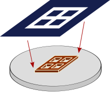
A photomask is an opaque plate with holes or transparencies that allow light to shine through in a defined pattern. They are commonly used in photolithography and the production of integrated circuits (ICs or "chips") in particular. Masks are used to produce a pattern on a substrate, normally a thin slice of silicon known as a wafer in the case of chip manufacturing. Several masks are used in turn, each one reproducing a layer of the completed design, and together they are known as a mask set.

In the 1960s, masks were created manually, normally using a material known as rubylith. As feature sizes shrank and wafer sizes grew, multiple copies of the design would be patterned onto the mask, allowing a single print run to produce many ICs. Making a mask of this sort became increasingly difficult as the complexity of the designs increased. This was solved by cutting the rubylith pattern at much larger sizes, often filling the walls of a room, and then optically shrinking them onto photographic film.
As complexity continued to grow, manual processing of any sort became difficult. This was solved with the introduction of the optical pattern generator which automated the process of producing the initial large-scale pattern, and the step-and-repeat cameras that automated the copying of the pattern into a multiple-IC mask. The intermediate masks are known as reticles, and were initially copied to production masks using the same photographic process. The initial stages produced by the generators have since been replaced by electron beam lithography and laser-driven systems. In these systems there may be no reticle, the masks can be generated directly from the original computerized design.
Mask materials have also changed over time. Initially, the rubylith was directly used as the mask. As feature size shrank the only way to properly focus the image was to place it in direct contact with the wafer. These contact aligners often lifted some of the photoresist off the wafer and the mask had to be discarded. This helped drive the adoption of reticles, which were used to produce thousands of masks. As the power of the lamps exposing the masks increased, film became subject to distortion due to heat, and was replaced by silver halide on soda glass. This same process led to the use of borosilicate and then quartz to control expansion, and from silver halide to chromium which has better opacity to the ultraviolet light used in the lithography process.
Overview

Lithographic photomasks are typically transparent fused silica blanks covered with a pattern defined with a chrome metal absorbing film. Photomasks are used at wavelengths of 365 nm, 248 nm, and 193 nm. Photomasks have also been developed for other forms of radiation such as 157 nm, 13.5 nm (EUV), X-ray, electrons, and ions; but these require entirely new materials for the substrate and the pattern film.
A set of photomasks, each defining a pattern layer in integrated circuit fabrication, is fed into a photolithography stepper or scanner, and individually selected for exposure. In double patterning techniques, a photomask would correspond to a subset of the layer pattern.
In photolithography for the mass production of integrated circuit devices, the more correct term is usually photoreticle or simply reticle. In the case of a photomask, there is a one-to-one correspondence between the mask pattern and the wafer pattern. This was the standard for the 1:1 mask aligners that were succeeded by steppers and scanners with reduction optics.[1] As used in steppers and scanners, the reticle commonly contains only one layer of the chip. (However, some photolithography fabrications utilize reticles with more than one layer patterned onto the same mask). The pattern is projected and shrunk by four or five times onto the wafer surface.[2] To achieve complete wafer coverage, the wafer is repeatedly "stepped" from position to position under the optical column until full exposure is achieved.
Features 150 nm or below in size generally require phase-shifting to enhance the image quality to acceptable values. This can be achieved in many ways. The two most common methods are to use an attenuated phase-shifting background film on the mask to increase the contrast of small intensity peaks, or to etch the exposed quartz so that the edge between the etched and unetched areas can be used to image nearly zero intensity. In the second case, unwanted edges would need to be trimmed out with another exposure. The former method is attenuated phase-shifting, and is often considered a weak enhancement, requiring special illumination for the most enhancement, while the latter method is known as alternating-aperture phase-shifting, and is the most popular strong enhancement technique.
As leading-edge semiconductor features shrink, photomask features that are 4× larger must inevitably shrink as well. This could pose challenges since the absorber film will need to become thinner, and hence less opaque.[3] A 2005 study by IMEC found that thinner absorbers degrade image contrast and therefore contribute to line-edge roughness, using state-of-the-art photolithography tools.[4] One possibility is to eliminate absorbers altogether and use "chromeless" masks, relying solely on phase-shifting for imaging.
The emergence of immersion lithography has a strong impact on photomask requirements. The commonly used attenuated phase-shifting mask is more sensitive to the higher incidence angles applied in "hyper-NA" lithography, due to the longer optical path through the patterned film.[5]
EUV photomasks work by reflecting light instead of blocking light.
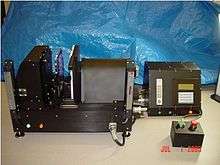
Photomasks are made by applying photoresist to a quartz substrate with chrome plating on one side and exposing it using a laser or an electron beam in a process called maskless lithography.[6] The photoresist is then developed and the unprotected areas with chrome are etched, and the remaining photoresist is removed. [7][8][9]
Mask error enhancement factor (MEEF)
Leading-edge photomasks (pre-corrected) images of the final chip patterns are magnified by four times. This magnification factor has been a key benefit in reducing pattern sensitivity to imaging errors. However, as features continue to shrink, two trends come into play: the first is that the mask error factor begins to exceed one, i.e., the dimension error on the wafer may be more than 1/4 the dimension error on the mask,[10] and the second is that the mask feature is becoming smaller, and the dimension tolerance is approaching a few nanometers. For example, a 25 nm wafer pattern should correspond to a 100 nm mask pattern, but the wafer tolerance could be 1.25 nm (5% spec), which translates into 5 nm on the photomask. The variation of electron beam scattering in directly writing the photomask pattern can easily well exceed this.[11][12]
Pellicles
The term "pellicle" is used to mean "film", "thin film", or "membrane." Beginning in the 1960s, thin film stretched on a metal frame, also known as a "pellicle", was used as a beam splitter for optical instruments. It has been used in a number of instruments to split a beam of light without causing an optical path shift due to its small film thickness. In 1978, Shea et al. at IBM patented a process to use the "pellicle" as a dust cover to protect a photomask or reticle. In the context of this entry, "pellicle" means "thin film dust cover to protect a photomask".
Particle contamination can be a significant problem in semiconductor manufacturing. A photomask is protected from particles by a pellicle – a thin transparent film stretched over a frame that is glued over one side of the photomask. The pellicle is far enough away from the mask patterns so that moderate-to-small sized particles that land on the pellicle will be too far out of focus to print. Although they are designed to keep particles away, pellicles become a part of the imaging system and their optical properties need to be taken into account. Pellicles material are Nitrocellulose and made for various Transmission Wavelengths.[13]

Leading commercial photomask manufacturers
The SPIE Annual Conference, Photomask Technology reports the SEMATECH Mask Industry Assessment which includes current industry analysis and the results of their annual photomask manufacturers survey. The following companies are listed in order of their global market share (2009 info):[14]
- Dai Nippon Printing
- Toppan Photomasks
- Photronics Inc
- Hoya Corporation
- Taiwan Mask Corporation
- Compugraphics
Major chipmakers such as Intel, Globalfoundries, IBM, NEC, TSMC, UMC, Samsung, and Micron Technology, have their own large maskmaking facilities or joint ventures with the abovementioned companies.
The worldwide photomask market was estimated as $3.2 billion in 2012[15] and $3.1 billion in 2013. Almost half of the market was from captive mask shops (in-house mask shops of major chipmakers).[16]
The costs of creating new mask shop for 180 nm processes were estimated in 2005 as $40 million, and for 130 nm - more than $100 million.[17]
The purchase price of a photomask, in 2006, could range from $250 to $100,000[18] for a single high-end phase-shift mask. As many as 30 masks (of varying price) may be required to form a complete mask set.
See also
- Integrated circuit layout design protection (or "Mask work")
- Mask inspection
- SMIF interface
- Nanochannel glass materials
- Stepping level
References
- Rizvi, Syed (2005). "1.3 The Technology History of Masks". Handbook of Photomask Manufacturing Technology. CRC Press. p. 728. ISBN 9781420028782.
- Lithography experts back higher magnification in photomasks to ease challenges // EETimes 2000
- Y. Sato et al., Proc. SPIE, vol. 4889, pp. 50-58 (2002).
- M. Yoshizawa et al., Proc. SPIE, vol. 5853, pp. 243-251 (2005)
- C. A. Mack et al., Proc. SPIE, vol. 5992, pp. 306-316 (2005)
- "ULTRA Semiconductor Laser Mask Writer | Heidelberg Instruments". www.himt.de.
- "Large Area Photomask Writer VPG+ | Heidelberg Instruments". www.himt.de.
- "Photomasks - Photolithography - Semiconductor Technology from A to Z - Halbleiter.org". www.halbleiter.org.
- "Compugraphics". Compugraphics.
- E. Hendrickx et al., Proc. SPIE 7140, 714007 (2008).
- C-J. Chen et al., Proc. SPIE 5256, 673 (2003).
- W-H. Cheng and J. Farnsworth, Proc. SPIE 6607, 660724 (2007).
- Chris A. Mack (November 2007). "Optical behavior of pellicles". Microlithography World. Retrieved 2008-09-13.
- Hughes, Greg; Henry Yun (2009-10-01). "Mask industry assessment: 2009". Proceedings of SPIE. 7488 (1): 748803-748803-13. doi:10.1117/12.832722. ISSN 0277-786X.
- Chamness, Lara (May 7, 2013). "Semiconductor Photomask Market: Forecast $3.5 Billion in 2014". SEMI Industry Research and Statistics. Retrieved 6 September 2014.
- Tracy, Dan; Deborah Geiger (April 14, 2014). "SEMI Reports 2013 Semiconductor Photomask Sales of $3.1 Billion". SEMI. Retrieved 6 September 2014.
- An Analysis of the Economics of Photomask Manufacturing Part – 1: The Economic Environment, Weber, February 9, 2005. Slide 6 "The Mask Shop's Perspective"
- Weber, C.M; Berglund, C.N.; Gabella, P. (13 November 2006). "Mask Cost and Profitability in Photomask Manufacturing: An Empirical Analysis" (PDF). IEEE Transactions on Semiconductor Manufacturing. 19 (4). doi:10.1109/TSM.2006.883577; page 23 table 1