Power integrity
Power integrity or PI is an analysis to check whether the desired voltage and current are met from source to destination. Today, power integrity plays a major role in the success and failure of new electronic products. There are several coupled aspects of PI: on the chip, in the chip package, on the circuit board, and in the system. Four main issues must be resolved to ensure power integrity at the printed circuit board level:[1]:615
- Keep the voltage ripple at the chips pads lower than the specification (e.g. less than +/-50 mV variation around 1V)
- Control ground bounce (also called synchronous switching noise, simultaneous switching noise, or simultaneous switching output (SSN or SSO))
- Control electromagnetic interference and maintain electromagnetic compatibility: the power distribution network is generally the largest set of conductors on the circuit board and therefore the largest (unwanted) antenna for emission and reception of noise.
- Maintaining a proper DC Voltage level at the load at high currents. A modern processor or field-programmable gate array can pull 1-100 Amps at sub-1V VDD levels with AC and DC margins in the tens of millivolts.[2][3] Very little DC voltage drop can thus be tolerated on the power distribution network.
Power distribution network

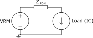
The current path from the power supply through the PCB and IC package to the die (consumer) is called the power distribution network.[4] Its role is to transfer the power to the consumers with little DC voltage drop, and to allow little ripple induced by dynamic current at the consumer(switching current). The DC drop occurs if there is too much resistance in the plane or power traces leading from the VRM to the consumer. This can be countered by raising the voltage on the VRM, or extending the "sense" point of the VRM to the consumer.
Dynamic current occur when the consumer switches its transistors, typically triggered by a clock. This dynamic current can be considerably larger than the static current (internal leakage) of the consumer. This fast current consumption can pull the voltage of the rail down, creating a voltage ripple. This change in current happens much faster than the VRM can react. The switching current must therefore be handled by decoupling capacitors.
The noise or voltage ripple must be handled differently depending on the frequency of operation. The highest frequencies must be handled on-die. This noise is decoupled by parasitic coupling in on the die, and capacitive coupling between metal layers. Frequencies above 50-100 MHz must be handled on the package, this is done by on package capacitors. Frequencies below 100 MHz are handled on the PCB by plane capacitance and using decoupling capacitors. Capacitors work on different frequencies depending on their type, capacitance and physical size. It is therefore necessary to utilize multiple capacitors of different sizes to ensure a low PDN impedance across the frequency range.[5] The physical size of the capacitors affect its parasitic inductance. The parasitic inductance creates impedance spikes at certain frequencies. (Physically) Smaller capacitors are therefore better. The placement of the capacitors is of varying importance depending on its frequency of operation. The smallest value capacitors should be as close as possible to the consumer to minimize the AC current loop area. Larger capacitors in the micro Farad range can be placed more or less anywhere.[6]
Target impedance
The target impedance is the impedance at which the ripple created by the dynamic current of the specific consumer is within the specified range. The target impedance is given by the following equation[7][8] In addition to the target impedance, it is important to know which frequencies it applies, and at which frequency the consumer package is responsible (this is specified in the datasheet of the specific consumer IC).
One usually use some form of simulation when designing the PDN to ensure that the PDN meets the target impedance. This can be done by SPICE simulation, chip vendor tools,[9] capacitor venor tools,[10] or by tools embedded in the EDA software.[11][12][13][14]


References
- Bogatin, Eric (13 July 2009). Signal and Power Integrity - Simplified. Pearson Education. ISBN 978-0-13-703503-8.
- "Simulating FPGA Power Integrity Using S-Parameter Models" (PDF). Xilinx. Retrieved 2018-03-18.
- "Virtex-7 T and XT FPGAs Data Sheet: DC and AC Switching Characteristics" (PDF). Xilinx. Retrieved 2018-03-18.
- "Fundamentals of Signal and Power Integrity" (PDF). Christian Schuster. Retrieved 2018-03-18.
- "Effective Power/Ground Plane Decoupling for PCB" (PDF). IBM. Retrieved 2018-03-18.
- "Introduction to Power Integrity" (PDF). PICOTEST, Keysight. Retrieved 2018-03-18.
- "Introduction to Power Integrity" (PDF). PICOTEST, Keysight. Retrieved 2018-03-18.
- "Designing for Power Integrity: Status, Challenges and Opportunities". IEEE. doi:10.1109/MEMC.2013.6623297. Cite journal requires
|journal=(help) - "Power Distribution Network". Altera. Retrieved 2018-03-18.
- "K-SIM". KEMET. Retrieved 2018-03-18.
- "CST PDN ANALYZER". Altium. Retrieved 2018-03-18.
- "HyperLynx Power Integrity". Mentor. Retrieved 2018-03-18.
- "Allegro Sigrity PI Base". Cadence. Retrieved 2018-03-18.
- "W2359EP PIPro Power Integrity EM Analysis Element". Keysight. Retrieved 2018-03-18.
Lee W. Ritchey (2003). Right the First Time—A Practical Handbook on High-speed PCB and System Design. SPEEDING EDGE. ISBN 978-0-9741936-0-1.