Integrated injection logic
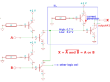
Integrated injection logic (IIL, I2L, or I2L) is a class of digital circuits built with multiple collector bipolar junction transistors (BJT).[1] When introduced it had speed comparable to TTL yet was almost as low power as CMOS, making it ideal for use in VLSI (and larger) integrated circuits. The gates can be made smaller with this logic family than with CMOS because complementary transistors are not needed. Although the logic voltage levels are very close (High: 0.7V, Low: 0.2V), I2L has high noise immunity because it operates by current instead of voltage. I2L was developed in 1971 by Siegfried K. Wiedmann and Horst H. Berger who originally called it merged-transistor logic (MTL).[2] A disadvantage of this logic family is that the gates draw power when not switching unlike with CMOS.

Construction

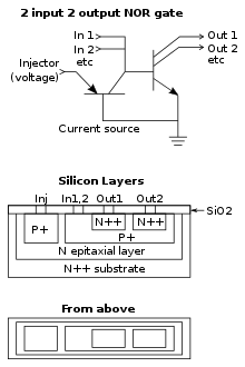
The I2L inverter gate is constructed with a PNP common base current source transistor and an NPN common emitter open collector inverter transistor. On a wafer, these two transistors are merged together. A small voltage (around 0.6 volts) is supplied to the emitter of the current source transistor to control the current supplied to the inverter transistor. Transistors are used for current sources on integrated circuits because they are much smaller than resistors.
Because the inverter is open collector, a wired AND operation may be performed by connecting an output from each of two or more gates together. Thus the fan-out of an output used in such a way is one. However, additional outputs may be produced by adding more collectors to the inverter transistor. The gates can be constructed very simply with just a single layer of interconnect metal.
In a discrete implementation of an I2L circuit, bipolar NPN transistors with multiple collectors can be replaced with multiple discrete 3-terminal NPN transistors connected in parallel having their bases connected together and their emitters connected likewise. Similarly, the merged PNP current injector transistor and the NPN inverter transistor can be implemented as separate discrete components. The current source transistor may be replaced with a resistor from the positive supply to the base of the inverter transistor, since discrete resistors are smaller and less expensive than discrete transistors.
Operation

The heart of an I2L circuit is the common emitter open collector inverter. Typically, an inverter consists of an NPN transistor with the emitter connected to ground and the base biased with a forward current from the current source. The input is supplied to the base as either a current sink (low logic level) or as a high-z floating condition (high logic level). The output of an inverter is at the collector. Likewise, it is either a current sink (low logic level) or a high-z floating condition (high logic level).
Like direct-coupled transistor logic, there is no resistor between the output (collector) of one NPN transistor and the input (base) of the following transistor.
To understand how the inverter operates, it is necessary to understand the current flow. If the bias current is shunted to ground (low logic level), the transistor turns off and the collector floats (high logic level). If the bias current is not shunted to ground because the input is high-z (high logic level), the bias current flows through the transistor to the emitter, switching on the transistor, and allowing the collector to sink current (low logic level). Because the output of the inverter can sink current but cannot source current, it is safe to connect the outputs of multiple inverters together to form a wired AND gate. When the outputs of two inverters are wired together, the result is a two-input NOR gate because the configuration (NOT A) AND (NOT B) is equivalent to NOT (A OR B) (per De Morgan's Theorem).
Due to internal parasitic capacitance in transistors, higher currents sourced into the base of the inverter transistor result in faster switching speeds, and since the voltage difference between high and low logic levels is smaller for I2L than other bipolar logic families (around 0.5 volts instead of around 3.3 or 5 volts), losses due to charging and discharging parasitic capacitances are minimized.
Usage
I2L is relatively simple to construct on an integrated circuit, and was commonly used before the advent of CMOS logic by companies such as Motorola (now Freescale)[3] and Texas Instruments (e.g. SBP0400). In 1975, Sinclair Radionics introduced one of the first consumer-grade digital watches, the Black Watch, which used I2L technology.[4] In the late 1970s, RCA used I²L in its CA3162 ADC 3 digit meter integrated circuit. In 1979, HP introduced a frequency measurement instrument based on a HP-made custom LSI chip that uses integrated injection logic (I2L) for low power consumption and high density, enabling portable battery operation, and also some emitter function logic (EFL) circuits where high speed is needed in its HP 5315A/B.[5]
References
- Hart, K.; Slob, A. (Oct 1972). "Integrated Injection Logic: A New Approach to LSI". IEEE Journal of Solid-State Circuits. 7 (5): 346–351. Bibcode:1972IJSSC...7..346H. doi:10.1109/jssc.1972.1052891.
- Siegfried K. Wiedmann, Horst H. Berger (1972). "Merged-transistor logic (MTL)-a low-cost bipolar logic concept". IEEE Journal of Solid-State Circuits. 7 (5): 340–346. Bibcode:1972IJSSC...7..340B. doi:10.1109/JSSC.1972.1052890.
- Jarrett, Robert (1978). "A monolithic speed-control micro-system for automotive applications". 1978 IEEE International Solid-State Circuits Conference. Digest of Technical Papers. IEEE. pp. 46–47. doi:10.1109/ISSCC.1978.1155757.
- "Clive Sinclair's 1982 Practical Computing Interview". Retrieved 21 June 2014.
- "HP memory project: Time, Frequency Standard & Counter"
Further reading
- Savard, John J. G. (2018) [2005]. "What Computers Are Made From". quadibloc. Archived from the original on 2018-07-02. Retrieved 2018-07-16.