Diode logic
Diode logic (DL), or diode-resistor logic (DRL), is the construction of Boolean logic gates from diodes. Diode logic was used extensively in the construction of early computers, where semiconductor diodes could replace bulky and costly active vacuum tube elements. The most common use for diode logic is in diode–transistor logic (DTL) integrated circuits that, in addition to diodes, include inverter logic for power gain and signal restoration.
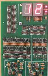
While diode logic has the advantage of simplicity, the lack of an amplifying stage in each gate limits its application. Not all logical functions can be implemented in diode logic alone; only the non-inverting logical AND and logical OR functions can be realized by diode gates. If several diode logic gates are cascaded, the voltage levels at each stage are significantly changed, so diode logic is normally limited to a single stage, though, in special designs, two-stage systems are sometimes achieved.
Simplifying assumptions
For illustration this discussion assumes idealized diodes that conduct in the forward direction with no voltage drop and do not conduct in the reverse direction. Logic design assumes two distinct levels of signals that are labeled 1 and 0. For positive logic the 1 represents the most positive level and 0 for the most negative level. For illustration in this discussion, positive logic 1 is represented by +6 volts and 0 volts represents logic 0. In binary logic the exact magnitude of the signal voltage is not critical and it is only necessary that 1 and 0 states be represented by detectably different voltage levels.
In these examples at least one input of every gate must be connected to a voltage level providing the defined logic 1 or logic 0 levels. If all the inputs are disconnected from any driving source the output signal is not confined to the correct voltage range.
Diode logic gates
In logic gates, logical functions are performed by parallel or series connected switches (such as relay contacts or insulated gate FETs like CMOS) controlled by logical inputs or parallel resistors or diodes which are passive components. Diode logic is implemented by diodes which exhibit low impedance when forward biased and a very high impedance when reverse biased. There are two kinds of diode logic gates - OR and AND. It is not possible to construct NOT (invert) diode gates because the invert function requires an active component such as a transistor.
OR logic gate
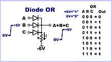
The image to the right shows a diode OR circuit. The diode symbol is an arrow showing the forward low impedance direction of current flow. All diodes have inputs on their anodes and their cathodes are connected together to drive the output. R is connected from the output to some negative voltage (-6 volts) to provide bias current for the diodes.
If all inputs A and B and C are at 0 volts (logic level 0), current flowing through R will pull the output voltage down until the diodes clamp the output. Since these diodes are treated as ideal, the output is clamped to 0 volts, which is logic level 0. If any input switches to a positive voltage (logic 1), current flowing through the now forward-biased diode will pull the output voltage up, providing a positive voltage at the output, a logic 1. Any positive voltage will represent a logic 1 state; the summing of currents through multiple diodes does not change the logic level. The other diodes are reverse biased and conduct no current.
If any input A OR B OR C is 1, the output will be 1. Only if all inputs, A and B and C are 0 will the output be 0. This is the definition of a logic OR. The truth table on the right of the image shows the output for all combinations of inputs.
This can be written as:
- A OR B OR C = OUTPUT
- or
- A+B+C=OUTPUT
In Boolean algebra the plus sign (+) is used to denote OR.
R can return to any negative voltage. If R is connected to 0 volts it will have no drive current available to drive the next circuit; practical diodes need a bias current. In a practical circuit, all signal levels, the value of R and its return voltage are chosen by the circuit designer to meet the design requirements.
AND logic gate
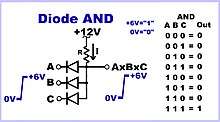
The diode AND is basically the same as the OR except it is turned upside down. The diodes are reversed so that the cathodes are connected to the inputs and the anodes are connected together to provide the output. R is connected to +12 volts to provide the forward bias current for the diodes and current for output drive.
If all inputs A AND B AND C are a positive voltage (+6 volts here), current flowing through R will pull the output positive till the diodes clamp the output to +6 volts, the logical 1 output level. If any input switches to 0 volts (logical 0 level), current flowing through the diode will pull the output voltage down to 0 volts. The other diodes would be reverse biased and conduct no current.
If input A or B or C is 0, the output will be 0. Only if all inputs, A AND B AND C are 1 will the output be 1. This is the definition of a logic AND. The truth table on the right of the image shows the output for all combinations of inputs.
This can be written as:
- A AND B AND C = OUTPUT
- or
- A×B×C=OUTPUT
(In Boolean algebra the multiplication symbol denotes AND.)
Similar to the diode OR, R can return to any voltage that is more positive than the logic level 1. If R is connected to a voltage equal to the 1 level it will have no drive current available to drive the next circuit. All signal levels, the value of R and its return voltage are options chosen by the circuit designer to meet the design requirements.
Negative logic
The assignment of 1 and 0 to the positive and negative signal levels respectively is an option of the logic designer using the AND or OR circuits. With this assignment it assumes that the logic is positive. It is just as likely that the assignment might be the reversed where 1 is the negative voltage and 0 is the positive voltage. This would be negative logic. Switching between positive and negative logic is commonly used to achieve a more efficient logic design.
In Boolean algebra it is recognized that a positive logic OR is a negative logic AND. Similarly a positive logic AND is a negative logic OR.
This relationship can easily be recognized by reading the above description of their operation. In the OR it stated, “Only if all inputs, A and B and C are 0 will the output be 0.” In negative logic each node at the lower voltage would become a logic 1, making the statement, “Only if all inputs, A AND B AND C are 1 will the output be 1.” That is the definition of an AND function.
Similarly for the AND it was stated, “If input A or B or C is 0 the output will be 0.” In negative logic each node at the lower voltage would become a logic 1, making the statement, “If input A OR B OR C is 1 the output will be 1.” That is the definition of an OR function.
The logical function of any arrangement of diodes can only be established if the representation of logic states by voltage levels is known. [1]
Diode logic with real diodes
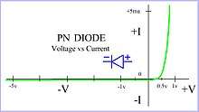
The above descriptions assumed an ideal diode with zero resistance in the forward direction and infinite resistance in the reverse direction. The circuit designer must concern himself with real diodes. The articles p-n diode and a less detailed article p-n junction describe the physics of the PN diode. After all the discussion of electrons, holes, majority and minority carriers etc. each come down to an equation that most directly relates to the circuit designer. The real PN diode actually has a voltage current characteristic similar to the curve on the right. A more specific definition can be found in the Shockley diode equation. The designer of a reliable diode logic circuit is usually limited to what the diode specification provides which is often less than the equation suggests. Typically the specification will primarily provide a maximum forward voltage drop at one or more forward currents and a reverse leakage current. It will also provide a maximum reverse voltage limited by zener or avalanche breakdown. Typical worst case specifications are shown below for both germanium and silicon PN diodes.
Germanium diode:
- Max forward voltage at 10 mA = 1 volt @ 0 to 85 °C
- Max reverse leakage current at 15 volts = 100 microamps @ 85 °C
Silicon diode:
- Max forward voltage at 10 mA = 1 volt @ 0 to 125 °C
- Max reverse leakage current at 15 volts = 1 microamps @ 85 °C
Effects of component manufacturing variations and temperature are usually included in these specifications.
More realistically the germanium forward voltage might be 0.25 to 0.4 volts but this is often not specified. The silicon leakage current might be much lower, possibly 1 to 100 nanoamps.
PN diodes also have transient behaviors that might be of concern with the design. The capacitance of a PN diode between anode and cathode is inversely proportional to the reverse voltage, growing as it approaches zero volts and into forward bias. There is also a recovery concern where the current will not decrease immediately when it is switched from forward bias to reverse bias. In the case of the diode OR if two or more of the inputs are at the 1 level and one switches to 0 it will cause a glitch or increase in current in the diodes that remain at 1. This can cause a short term dip in the output voltage. In practice if the diode logic gate drives a transistor inverter, as it usually does, and the diode and transistor are of similar construction the transistor will have a similar base collector capacitance that is amplified by the transistor gain so that it will be too slow to pass the glitch. Only when the diode is of a much slower construction will it become any concern at all. In one unusual design small selenium diode discs were used with germanium transistors. The recovery time of the very slow selenium diodes caused a glitch on the inverter output. It was fixed by placing a selenium diode across the base emitter junction of the transistor making it “think” it was a selenium transistor (if there could ever be one).
Early diode logic with transistor inverter
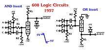
Up until 1952, IBM manufactured transistors by modifying off-the-shelf germanium diodes, after which they had their own alloy-junction transistor manufacturing plant at Poughkeepsie.[3][4] In the mid 1950s diode logic was used in the IBM 608 which was the first all-transistorized computer in the world. The image on the right shows two basic logic circuits used on 608 cards. A single card would hold four two-way circuits or three three-way or one eight-way. All input and output signals were compatible. The circuits were capable of reliably switching pulses as narrow as one microsecond.
The designers of the 1962 D-17B used diode-resistor logic as much as possible, to minimize the number of transistors used.
Restoration
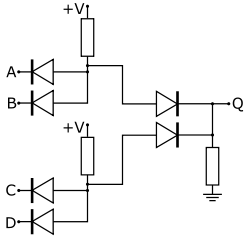
Digital logic implemented by active elements is characterized by signal restoration. True and false or 1 and 0 are represented by two specific voltage levels. If the inputs to a digital logic gate is close to their respective levels, the output will be closer or exactly equal to its desired level. Active logic gates may be integrated in large numbers because each gate tends to remove noise at its input. Diode logic gates are implemented by passive elements; so, they have two restoration problems.
- Forward voltage drop
- The first restoration problem of diode logic is that there is a voltage drop VF about 0.6 V across the forward-biased diode. This voltage is added to or subtracted from the input of every gate so that it accumulates when diode gates are cascaded. In an OR gate, VF decreases the high voltage level (the logical 1) while in an AND gate, it increases the low voltage level (the logical 0). The feasible number of logic stages thus depends on the voltage drop and difference between the high and low voltages.
- Source resistance
- Another problem of diode logic is the internal resistance of the input voltage sources. Together with the gate resistor, it constitutes a voltage divider that causes deviations in voltage levels. In an OR gate, the source resistance decreases the high voltage level (the logical 1) while in an AND gate, it increases the low voltage level (the logical 0). In the cascaded AND-OR diode gates in the picture on the right, the AND high output voltages are decreased because of the internal voltage drops across the AND pull-up resistances.[5]
Applications
Diode logic gates are used to build diode–transistor logic (DTL) gates as integrated circuits.
The outputs of conventional ICs (with complementary output drive stages) are never directly connected together since they act as voltage sources. However, diodes can be used to combine two or more digital (high/low) outputs from an IC such as a counter. This wired logic connection can be a useful way of producing simple logic functions without using additional logic gates.[6]
Most circuit families are designed to have compatible inputs and outputs depending on these signal levels to achieve reliable performance. Adding diode logic will degrade the signal level and result in poor noise rejection and possible failure.
Tunnel diodes
During the 1960s the use of tunnel diodes in logic circuits was an active research topic. When compared to transistor logic gates of the time, the tunnel diode offered much higher speeds. Unlike other diode types, the tunnel diode offered the possibility of amplification of signals at each stage. The operating principles of a tunnel diode logic rely on biasing of the tunnel diode and supply of current from inputs over a threshold current, to switch the diode between two states. Consequently, tunnel diode logic circuits required a means to reset the diode after each logical operation. A simple tunnel diode gate offered little isolation between inputs and outputs and had low fan in and fan out. More complex gates, with additional tunnel diodes and bias power supplies, overcame some of these limitations. [7] Advances in discrete and integrated circuit transistor speed and the more nearly unilateral nature of transistor amplifiers overtook the tunnel diode gate and it is no longer used in modern computers.
See also
References
- United States Dept. of the Army, Communications-electronics Fundamentals: Digital Computers Field manual FM 11-72 1978, pages 3-17 through 3-22
- IBM Customer Manual of Instruction: Transistor Component Circuits, p. 20, IBM, 1960.
- Emerson W. Pugh, Lyle R. Johnson, John H. Palmer, IBM's 360 and Early 370 Systems, pp. 33-34, MIT Press, 1991 ISBN 0262161230.
- Bo Lojek, History of Semiconductors, pp. 60-61, Springer Science & Business Media, 2007 ISBN 3540342583.
- Diode logic
- Integrated Circuits (Chips)
- Tunnel Diodes for Switching and Microwave Applications Technical Manual TD-30, RCA 1963, (3rd Chapter) Switching
External links
| Wikimedia Commons has media related to Diode logic. |