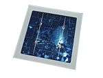
Multi-junction solar cell
Multi-junction (MJ) solar cells are solar cells with multiple p–n junctions made of different semiconductor materials. Each material's p-n junction will produce electric current in response to different wavelengths of light. The use of multiple semiconducting materials allows the absorbance of a broader range of wavelengths, improving the cell's sunlight to electrical energy conversion efficiency.
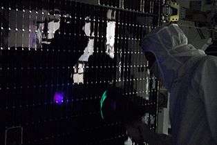
Traditional single-junction cells have a maximum theoretical efficiency of 33.16%.[2] Theoretically, an infinite number of junctions would have a limiting efficiency of 86.8% under highly concentrated sunlight.[3]
Currently, the best lab examples of traditional crystalline silicon (c-Si) solar cells have efficiencies between 20% and 25%,[4] while lab examples of multi-junction cells have demonstrated performance over 46% under concentrated sunlight.[5][6][7] Commercial examples of tandem cells are widely available at 30% under one-sun illumination,[8][9] and improve to around 40% under concentrated sunlight. However, this efficiency is gained at the cost of increased complexity and manufacturing price. To date, their higher price and higher price-to-performance ratio have limited their use to special roles, notably in aerospace where their high power-to-weight ratio is desirable. In terrestrial applications, these solar cells are emerging in concentrator photovoltaics (CPV), with a growing number of installations around the world.[10]
Tandem fabrication techniques have been used to improve the performance of existing designs. In particular, the technique can be applied to lower cost thin-film solar cells using amorphous silicon, as opposed to conventional crystalline silicon, to produce a cell with about 10% efficiency that is lightweight and flexible. This approach has been used by several commercial vendors,[11] but these products are currently limited to certain niche roles, like roofing materials.
Description
Basics of solar cells
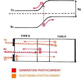
Traditional photovoltaic cells are commonly composed of doped silicon with metallic contacts deposited on the top and bottom. The doping is normally applied to a thin layer on the top of the cell, producing a p-n junction with a particular bandgap energy, Eg.
Photons that hit the top of the solar cell are either reflected or transmitted into the cell. Transmitted photons have the potential to give their energy, hν, to an electron if hν ≥ Eg, generating an electron-hole pair.[13] In the depletion region, the drift electric field Edrift accelerates both electrons and holes towards their respective n-doped and p-doped regions (up and down, respectively). The resulting current Ig is called the generated photocurrent. In the quasi-neutral region, the scattering electric field Escatt accelerates holes (electrons) towards the p-doped (n-doped) region, which gives a scattering photocurrent Ipscatt (Inscatt). Consequently, due to the accumulation of charges, a potential V and a photocurrent Iph appear. The expression for this photocurrent is obtained by adding generation and scattering photocurrents: Iph = Ig + Inscatt + Ipscatt.
The J-V characteristics (J is current density, i.e. current per unit area) of a solar cell under illumination are obtained by shifting the J-V characteristics of a diode in the dark downward by Iph. Since solar cells are designed to supply power and not absorb it, the power P = V·Iph must be negative. Hence, the operating point (Vm, Jm) is located in the region where V>0 and Iph<0, and chosen to maximize the absolute value of the power |P|.[14]
Loss mechanisms
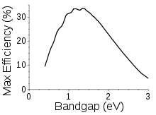
The theoretical performance of a solar cell was first studied in depth in the 1960s, and is today known as the Shockley–Queisser limit. The limit describes several loss mechanisms that are inherent to any solar cell design.
The first are the losses due to blackbody radiation, a loss mechanism that affects any material object above absolute zero. In the case of solar cells at standard temperature and pressure, this loss accounts for about 7% of the power. The second is an effect known as "recombination", where the electrons created by the photoelectric effect meet the electron holes left behind by previous excitations. In silicon, this accounts for another 10% of the power.
However, the dominant loss mechanism is the inability of a solar cell to extract all of the power in the light, and the associated problem that it cannot extract any power at all from certain photons. This is due to the fact that the photons must have enough energy to overcome the bandgap of the material.
If the photon has less energy than the bandgap, it is not collected at all. This is a major consideration for conventional solar cells, which are not sensitive to most of the infrared spectrum, although that represents almost half of the power coming from the sun. Conversely, photons with more energy than the bandgap, say blue light, initially eject an electron to a state high above the bandgap, but this extra energy is lost through collisions in a process known as "relaxation". This lost energy turns into heat in the cell, which has the side-effect of further increasing blackbody losses.[15]
Combining all of these factors, the maximum efficiency for a single-bandgap material, like conventional silicon cells, is about 34%. That is, 66% of the energy in the sunlight hitting the cell will be lost. Practical concerns further reduce this, notably reflection off the front surface or the metal terminals, with modern high-quality cells at about 22%.
Lower, also called narrower, bandgap materials will convert longer wavelength, lower energy photons. Higher, or wider bandgap materials will convert shorter wavelength, higher energy light. An analysis of the AM1.5 spectrum, shows the best balance is reached at about 1.1 eV (about 1100 nm, in the near infrared), which happens to be very close to the natural bandgap in silicon and a number of other useful semiconductors.
Multi-junction cells
Cells made from multiple materials layers can have multiple bandgaps and will therefore respond to multiple light wavelengths, capturing and converting some of the energy that would otherwise be lost to relaxation as described above.
For instance, if one had a cell with two bandgaps in it, one tuned to red light and the other to green, then the extra energy in green, cyan and blue light would be lost only to the bandgap of the green-sensitive material, while the energy of the red, yellow and orange would be lost only to the bandgap of the red-sensitive material. Following analysis similar to those performed for single-bandgap devices, it can be demonstrated that the perfect bandgaps for a two-gap device are at 0.77 eV and 1.70 eV. [16]
Conveniently, light of a particular wavelength does not interact strongly with materials that are of bigger bandgap. This means that you can make a multi-junction cell by layering the different materials on top of each other, shortest wavelengths (biggest bandgap) on the "top" and increasing through the body of the cell. As the photons have to pass through the cell to reach the proper layer to be absorbed, transparent conductors need to be used to collect the electrons being generated at each layer.
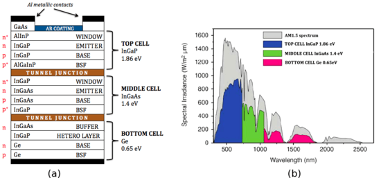
Producing a tandem cell is not an easy task, largely due to the thinness of the materials and the difficulties extracting the current between the layers. The easy solution is to use two mechanically separate thin film solar cells and then wire them together separately outside the cell. This technique is widely used by amorphous silicon solar cells, Uni-Solar's products use three such layers to reach efficiencies around 9%. Lab examples using more exotic thin-film materials have demonstrated efficiencies over 30%.[17]
The more difficult solution is the "monolithically integrated" cell, where the cell consists of a number of layers that are mechanically and electrically connected. These cells are much more difficult to produce because the electrical characteristics of each layer have to be carefully matched. In particular, the photocurrent generated in each layer needs to be matched, otherwise electrons will be absorbed between layers. This limits their construction to certain materials, best met by the III-V semiconductors.[17]
Material choice
The choice of materials for each sub-cell is determined by the requirements for lattice-matching, current-matching, and high performance opto-electronic properties.
For optimal growth and resulting crystal quality, the crystal lattice constant a of each material must be closely matched, resulting in lattice-matched devices. This constraint has been relaxed somewhat in recently developed metamorphic solar cells which contain a small degree of lattice mismatch. However, a greater degree of mismatch or other growth imperfections can lead to crystal defects causing a degradation in electronic properties.
Since each sub-cell is connected electrically in series, the same current flows through each junction. The materials are ordered with decreasing bandgaps, Eg, allowing sub-bandgap light (hc/λ < e·Eg) to transmit to the lower sub-cells. Therefore, suitable bandgaps must be chosen such that the design spectrum will balance the current generation in each of the sub-cells, achieving current matching. Figure C(b) plots spectral irradiance E(λ), which is the source power density at a given wavelength λ. It is plotted together with the maximum conversion efficiency for every junction as a function of the wavelength, which is directly related to the number of photons available for conversion into photocurrent.
Finally, the layers must be electrically optimal for high performance. This necessitates usage of materials with strong absorption coefficients α(λ), high minority carrier lifetimes τminority, and high mobilities µ.[18]
The favorable values in the table below justify the choice of materials typically used for multi-junction solar cells: InGaP for the top sub-cell (Eg = 1.8 − 1.9 eV), InGaAs for the middle sub-cell (Eg = 1.4 eV), and Germanium for the bottom sub-cell (Eg = 0.67 eV). The use of Ge is mainly due to its lattice constant, robustness, low cost, abundance, and ease of production.
Because the different layers are closely lattice-matched, the fabrication of the device typically employs metal-organic chemical vapor deposition (MOCVD). This technique is preferable to the molecular beam epitaxy (MBE) because it ensures high crystal quality and large scale production.[14]
| Material | Eg, eV | a, nm | absorption (λ = 0.8 μm), 1/µm |
µn, cm2/(V·s) | τp, µs | Hardness (Mohs) |
α, µm/K | S, m/s |
|---|---|---|---|---|---|---|---|---|
| c-Si | 1.12 | 0.5431 | 0.102 | 1400 | 1 | 7 | 2.6 | 0.1–60 |
| InGaP | 1.86 | 0.5451 | 2 | 500 | – | 5 | 5.3 | 50 |
| GaAs | 1.4 | 0.5653 | 0.9 | 8500 | 3 | 4–5 | 6 | 50 |
| Ge | 0.65 | 0.5657 | 3 | 3900 | 1000 | 6 | 7 | 1000 |
| InGaAs | 1.2 | 0.5868 | 30 | 1200 | – | – | 5.66 | 100–1000 |
Structural elements
Metallic contacts
The metallic contacts are low-resistivity electrodes that make contact with the semiconductor layers. They are often aluminum. This provides an electrical connection to a load or other parts of a solar cell array. They are usually on two sides of the cell. And are important to be on the back face so that shadowing on the lighting surface is reduced.
Anti-reflective coating
Anti-reflective (AR) coating is generally composed of several layers in the case of MJ solar cells. The top AR layer has usually a NaOH surface texturation with several pyramids in order to increase the transmission coefficient T, the trapping of the light in the material (because photons cannot easily get out the MJ structure due to pyramids) and therefore, the path length of photons in the material.[12] On the one hand, the thickness of each AR layer is chosen to get destructive interferences. Therefore, the reflection coefficient R decreases to 1%. In the case of two AR layers L1 (the top layer, usually SiO
2) and L2 (usually TiO
2), there must be to have the same amplitudes for reflected fields and nL1dL1 = 4λmin,nL2dL2 = λmin/4 to have opposite phase for reflected fields.[19] On the other hand, the thickness of each AR layer is also chosen to minimize the reflectance at wavelengths for which the photocurrent is the lowest. Consequently, this maximizes JSC by matching currents of the three subcells.[20] As example, because the current generated by the bottom cell is greater than the currents generated by the other cells, the thickness of AR layers is adjusted so that the infrared (IR) transmission (which corresponds to the bottom cell) is degraded while the ultraviolet transmission (which corresponds to the top cell) is upgraded. Particularly, an AR coating is very important at low wavelengths because, without it, T would be strongly reduced to 70%.
Tunnel junctions
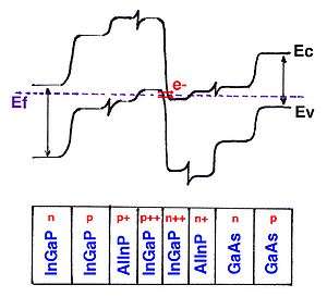
The main goal of tunnel junctions is to provide a low electrical resistance and optically low-loss connection between two subcells.[21] Without it, the p-doped region of the top cell would be directly connected with the n-doped region of the middle cell. Hence, a pn junction with opposite direction to the others would appear between the top cell and the middle cell. Consequently, the photovoltage would be lower than if there would be no parasitic diode. In order to decrease this effect, a tunnel junction is used.[22] It is simply a wide band gap, highly doped diode. The high doping reduces the length of the depletion region because
Hence, electrons can easily tunnel through the depletion region. The J-V characteristic of the tunnel junction is very important because it explains why tunnel junctions can be used to have a low electrical resistance connection between two pn junctions. Figure D shows three different regions: the tunneling region, the negative differential resistance region and the thermal diffusion region. The region where electrons can tunnel through the barrier is called the tunneling region. There, the voltage must be low enough so that energy of some electrons who are tunneling is equal to energy states available on the other side of the barrier. Consequently, current density through the tunnel junction is high (with maximum value of , the peak current density) and the slope near the origin is therefore steep. Then, the resistance is extremely low and consequently, the voltage too.[23] This is why tunnel junctions are ideal for connecting two pn junctions without having a voltage drop. When voltage is higher, electrons cannot cross the barrier because energy states are no longer available for electrons. Therefore, the current density decreases and the differential resistance is negative. The last region, called thermal diffusion region, corresponds to the J-V characteristic of the usual diode:
In order to avoid the reduction of the MJ solar cell performances, tunnel junctions must be transparent to wavelengths absorbed by the next photovoltaic cell, the middle cell, i.e. EgTunnel > EgMiddleCell.
Window layer and back-surface field
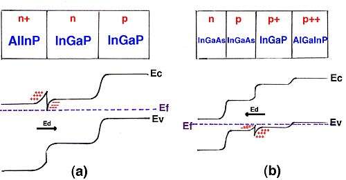
A window layer is used in order to reduce the surface recombination velocity S. Similarly, a back-surface field (BSF) layer reduces the scattering of carriers towards the tunnel junction. The structure of these two layers is the same: it is a heterojunction which catches electrons (holes). Indeed, despite the electric field Ed, these cannot jump above the barrier formed by the heterojunction because they don't have enough energy, as illustrated in figure E. Hence, electrons (holes) cannot recombine with holes (electrons) and cannot diffuse through the barrier. By the way, window and BSF layers must be transparent to wavelengths absorbed by the next pn junction i.e. EgWindow > EgEmitter and EgBSF > EgEmitter. Furthermore, the lattice constant must be close to the one of InGaP and the layer must be highly doped (n ≥ 1018 cm−3).[24]
J-V characteristic
For maximum efficiency, each subcell should be operated at its optimal J-V parameters, which are not necessarily equal for each subcell. If they are different, the total current through the solar cell is the lowest of the three. By approximation,[25] it results in the same relationship for the short-circuit current of the MJ solar cell: JSC = min (JSC1, JSC2, JSC3) where JSCi(λ) is the short-circuit current density at a given wavelength λ for the subcell i.
Because of the impossibility to obtain JSC1, JSC2, JSC3 directly from the total J-V characteristic, the quantum efficiency QE(λ) is utilized. It measures the ratio between the amount of electron-hole pairs created and the incident photons at a given wavelength λ. Let φi(λ) be the photon flux of corresponding incident light in subcell iandQEi(λ) be the quantum efficiency of the subcell i. By definition, this equates to:[26]
The value of is obtained by linking it with the absorption coefficient , i.e. the number of photons absorbed per unit of length by a material. If it is assumed that each photon absorbed by a subcell creates an electron/hole pair (which is a good approximation), this leads to:[24]
- where di is the thickness of the subcell i and is the percentage of incident light which is not absorbed by the subcell i.
Similarly, because
- , the following approximation can be used: .
The values of are then given by the J-V diode equation:
Theoretical limiting efficiency
We can estimate the limiting efficiency of ideal infinite multi-junction solar cells using the graphical quantum-efficiency (QE) analysis invented by C. H. Henry.[27]
To fully take advantage of Henry's method, the unit of the AM1.5 spectral irradiance should be converted to that of photon flux (i.e., number of photons/m2/s). To do that, it is necessary to carry out an intermediate unit conversion from the power of electromagnetic radiation incident per unit area per photon energy to the photon flux per photon energy (i.e., from [W/m2/eV] to [number of photons/m2/s/eV]). For this intermediate unit conversion, the following points have to be considered: A photon has a distinct energy which is defined as follows.
(1): Eph = h∙f = h∙(c/λ)
where Eph is photon energy, h is Planck's constant (h = 6.626*10−34 [J∙s]), c is speed of light (c = 2.998*108 [m/s]), f is frequency [1/s], and λ is wavelength [nm].
Then the photon flux per photon energy, dnph/dhν, with respect to certain irradiance E [W/m2/eV] can be calculated as follows.
(2): = E/{h∙(c/λ)} = E[W/(m2∙eV)]∙λ∙(10−9 [m])/(1.998∙10−25 [J∙s∙m/s]) = E∙λ∙5.03∙1015 [(# of photons)/(m2∙s∙eV)]
As a result of this intermediate unit conversion, the AM1.5 spectral irradiance is given in unit of the photon flux per photon energy, [number of photons/m2/s/eV], as shown in Figure 1.
 Figure 1. Photon flux per photon energy from standard solar energy spectrum (AM of 1.5).
Based on the above result from the intermediate unit conversion, we can derive the photon flux by numerically integrating the photon flux per photon energy with respect to photon energy. The numerically integrated photon flux is calculated using the Trapezoidal rule, as follows.
(3):
As a result of this numerical integration, the AM1.5 spectral irradiance is given in unit of the photon flux, [number of photons/m2/s], as shown in Figure 2.
 Figure 2. Photon flux from standard solar energy spectrum (AM of 1.5).
There are no photon flux data in the small photon energy range from 0 eV to 0.3096 eV because the standard (AM1.5) solar energy spectrum for hν < 0.31 eV are not available. Regardless of this data unavailability, however, the graphical QE analysis can be done using the only available data with a reasonable assumption that semiconductors are opaque for photon energies greater than their bandgap energy, but transparent for photon energies less than their bandgap energy. This assumption accounts for the first intrinsic loss in the efficiency of solar cells, which is caused by the inability of single-junction solar cells to properly match the broad solar energy spectrum. However, the current graphical QE analysis still cannot reflect the second intrinsic loss in the efficiency of solar cells, radiative recombination. To take the radiative recombination into account, we need to evaluate the radiative current density, Jrad, first. According to Shockley and Queisser method,[28] Jrad can be approximated as follows.
(4):
(5):
where Eg is in electron volts and n is evaluated to be 3.6, the value for GaAs. The incident absorbed thermal radiation Jth is given by Jrad with V = 0.
(6):
The current density delivered to the load is the difference of the current densities due to absorbed solar and thermal radiation and the current density of radiation emitted from the top surface or absorbed in the substrate. Defining Jph = enph, we have
(7): J = Jph + Jth − Jrad
The second term, Jth, is negligible compared to Jph for all semiconductors with Eg. ≥ 0.3 eV, as can be shown by evaluation of the above Jth equation. Thus, we will neglect this term to simplify the following discussion. Then we can express J as follows.
(8):
The open-circuit voltage is found by setting J = 0.
(9):
The maximum power point (Jm, Vm) is found by setting the derivative . The familiar result of this calculation is
(10):
(11):
Finally, the maximum work (Wm) done per absorbed photon, Wm is given by
(12):
Combining the last three equations, we have
(13):
Using the above equation, Wm (red line) is plotted in Figure 3 for different values of Eg (or nph).
 Figure 3. Maximum work by ideal infinite multi-junction solar cells under standard AM1.5 spectral irradiance.
Now, we can fully use Henry's graphical QE analysis, taking into account the two major intrinsic losses in the efficiency of solar cells. The two main intrinsic losses are radiative recombination, and the inability of single junction solar cells to properly match the broad solar energy spectrum. The shaded area under the red line represents the maximum work done by ideal infinite multi-junction solar cells. Hence, the limiting efficiency of ideal infinite multi-junction solar cells is evaluated to be 68.8% by comparing the shaded area defined by the red line with the total photon-flux area determined by the black line. (This is why this method is called "graphical" QE analysis.) Although this limiting efficiency value is consistent with the values published by Parrott and Vos in 1979: 64% and 68.2% respectively,[29][30] there is a small gap between the estimated value in this report and literature values. This minor difference is most likely due to the different ways how to approximate the photon flux from 0 eV to 0.3096 eV. Here, we approximated the photon flux from 0 eV to 0.3096 eV as the same as the photon flux at 0.31 eV.
Materials
The majority of multi-junction cells that have been produced to date use three layers (although many tandem a-Si:H/mc-Si modules have been produced and are widely available). However, the triple junction cells require the use of semiconductors that can be tuned to specific frequencies, which has led to most of them being made of gallium arsenide (GaAs) compounds, often germanium for the bottom-, GaAs for the middle-, and GaInP2 for the top-cell.
Gallium arsenide substrate
Dual junction cells can be made on Gallium arsenide wafers. Alloys of Indium gallium phosphide in the range In.5Ga.5P through In.53Ga.47P serve as the high band gap alloy. This alloy range provides for the ability to have band gaps in the range of 1.92eV to 1.87eV. The lower GaAs junction has a band gap of 1.42eV.
Germanium substrate
Triple junction cells consisting of indium gallium phosphide (InGaP), gallium arsenide (GaAs) or indium gallium arsenide (InGaAs) and germanium (Ge) can be fabricated on germanium wafers. Early cells used straight gallium arsenide in the middle junction. Later cells have utilized In0.015Ga0.985As, due to the better lattice match to Ge, resulting in a lower defect density.
Due to the huge band gap difference between GaAs (1.42eV), and Ge (0.66eV), the current match is very poor, with the Ge junction operated significantly current limited.
Current efficiencies for commercial InGaP/GaAs/Ge cells approach 40% under concentrated sunlight.[31][32] Lab cells (partly using additional junctions between the GaAs and Ge junction) have demonstrated efficiencies above 40%.[33]
Indium phosphide substrate
Indium phosphide may be used as a substrate to fabricate cells with band gaps between 1.35eV and 0.74eV. Indium Phosphide has a band gap of 1.35eV. Indium gallium arsenide (In0.53Ga0.47As) is lattice matched to Indium Phosphide with a band gap of 0.74eV. A quaternary alloy of Indium gallium arsenide phosphide can be lattice matched for any band gap in between the two.
Indium phosphide-based cells have the potential to work in tandem with gallium arsenide cells. The two cells can be optically connected in series (with the InP cell below the GaAs cell), or in parallel through the use of spectra splitting using a Dichroic filter.
Indium gallium nitride substrate
Indium gallium nitride (InGaN) is a semiconductor material made of a mix of gallium nitride (GaN) and indium nitride (InN). It is a ternary group III/V direct bandgap semiconductor. Its bandgap can be tuned by varying the amount of indium in the alloy from 0.7 eV to 3.4 eV, thus making it an ideal material for solar cells.[34] However, its conversion efficiencies because of technological factors unrelated to bandgap are still not high enough to be competitive in the market.[35][36]
Performance improvements
Structure
Many MJ photovoltaic cells use III-V semiconductor materials. GaAsSb-based heterojunction tunnel diodes, instead of conventional InGaP highly doped tunnel diodes described above, have a lower tunneling distance. Indeed, in the heterostructure formed by GaAsSb and InGaAs, the valence band of GaAsSb is higher than the valence band of the adjoining p-doped layer.[22] Consequently, the tunneling distance dtunnel is reduced and so the tunneling current, which exponentially depends of dtunnel, is increased. Hence, the voltage is lower than that of the InGaP tunnel junction. GaAsSb heterojunction tunnel diodes offer other advantages. The same current can be achieved by using a lower doping.[37] Secondly, because the lattice constant is larger for GaAsSb than Ge, one can use a wider range of materials for the bottom cell because more materials are lattice-matched to GaAsSb than to Ge.[22]
Chemical components can be added to some layers. Adding about one percent of Indium in each layer better matches lattice constants of the different layers.[38] Without it, there is about 0.08 percent of mismatching between layers, which inhibits performance. Adding aluminium to the top cell increases its band gap to 1.96 eV,[38] covering a larger part of the solar spectrum and obtain a higher open-circuit voltage VOC.
The theoretical efficiency of MJ solar cells is 86.8% for an infinite number of pn junctions,[14] implying that more junctions increase efficiency. The maximum theoretical efficiency is 37, 50, 56, 72% for 1, 2, 3, 36 pn junctions, respectively, with the number of junctions increasing exponentially to achieve equal efficiency increments.[24] The exponential relationship implies that as the cell approaches the limit of efficiency, the increase cost and complexity grow rapidly. Decreasing the thickness of the top cell increases the transmission coefficient T.[24]
An InGaP hetero-layer between the p-Ge layer and the InGaAs layer can be added in order to create automatically the n-Ge layer by scattering during MOCVD growth and increase significantly the quantum efficiency QE(λ) of the bottom cell.[38] InGaP is advantageous because of its high scattering coefficient and low solubility in Ge.
Currently, there are several commercial (nonperovskite) multi-junction technologies including tandems and triple- and quadruple-junction modules that typically use III to V semiconductors, with promising power conversion efficiency that rival and even outperform the benchmark silicon solar cells.[39]
Spectral variations
Solar spectrum at the Earth surface changes constantly depending on the weather and sun position. This results in the variation of φ(λ), QE(λ), α(λ) and thus the short-circuit currents JSCi. As a result, the current densities Ji are not necessarily matched and the total current becomes lower. These variations can be quantified using the average photon energy (APE) which is the ratio between the spectral irradiance G(λ) (the power density of the light source in a specific wavelength λ) and the total photon flux density. It can be shown that a high (low) value for APE means low (high) wavelengths spectral conditions and higher (lower) efficiencies.[40] Thus APE is a good indicator for quantifying the effects of the solar spectrum variations on performances and has the added advantage of being independent of the device structure and the absorption profile of the device.[40]
Use of light concentrators
Light concentrators increase efficiencies and reduce the cost/efficiency ratio. The three types of light concentrators in use are refractive lenses like Fresnel lenses, reflective dishes (parabolic or cassegraine), and light guide optics. Thanks to these devices, light arriving on a large surface can be concentrated on a smaller cell. The intensity concentration ratio (or “suns”) is the average intensity of the focused light divided by 1 kW/m2 (reasonable value related to solar constant). If its value is X then the MJ current becomes X higher under concentrated illumination.[41][42]
Using concentrations on the order of 500 to 1000, meaning that a 1 cm2 cell can use the light collected from 0.1 m2 (as 1 m2 equal 10000 cm2), produces the highest efficiencies seen to date. Three-layer cells are fundamentally limited to 63%, but existing commercial prototypes have already demonstrated over 40%.[43][44] These cells capture about 2/3 of their theoretical maximum performance, so assuming the same is true for a non-concentrated version of the same design, one might expect a three-layer cell of 30% efficiency. This is not enough of an advantage over traditional silicon designs to make up for their extra production costs. For this reason, almost all multi-junction cell research for terrestrial use is dedicated to concentrator systems, normally using mirrors or fresnel lenses.
Using a concentrator also has the added benefit that the number of cells needed to cover a given amount of ground area is greatly reduced. A conventional system covering 1 m2 would require 625 16 cm2 cells, but for a concentrator system only a single cell is needed, along with a concentrator. The argument for concentrated Multi-junction cells has been that the high cost of the cells themselves would be more than offset by the reduction in total number of cells. However, the downside of the concentrator approach is that efficiency drops off very quickly under lower lighting conditions. In order to maximize its advantage over traditional cells and thus be cost competitive, the concentrator system has to track the sun as it moves to keep the light focused on the cell and maintain maximum efficiency as long as possible. This requires a solar tracker system, which increases yield, but also cost.
Fabrication
As of 2014 multi-junction cells were expensive to produce, using techniques similar to semiconductor device fabrication, usually metalorganic vapour phase epitaxy but on "chip" sizes on the order of centimeters.
A new technique was announced that year that allowed such cells to use a substrate of glass or steel, lower-cost vapors in reduced quantities that was claimed to offer costs competitive with conventional silicon cells.[45]
Comparison with other technologies
There are four main categories of photovoltaic cells: conventional mono and multi crystalline silicon (c-Si) cells, thin film solar cells (a-Si, CIGS and CdTe), and multi-junction (MJ) solar cells. The fourth category, emerging photovoltaics, contains technologies that are still in the research or development phase and are not listed in the table below.
| Categories | Technology | η (%) | VOC (V) | ISC (A) | W/m2 | t (µm) | Refs |
|---|---|---|---|---|---|---|---|
| Crystalline silicon cells | Monocrystalline | 24.7 | 0.5 | 0.8 | 63 | 100 | |
| Polysilicon | 20.3 | 0.615 | 8.35 | 211 | 200 | ||
| Thin film solar cells |
Amorphous silicon | 11.1 | 0.63 | 0.089 | 33 | 1 | |
| CdTe | 16.5 | 0.86 | 0.029 | – | 5 | ||
| CIGS | 19.5 | – | – | – | 1 | ||
| Multi-junction cells | MJ | 40.7 | 2.6 | 1.81 | 476 | 140 |
MJ solar cells and other photovoltaic devices have significant differences (see the table above). Physically, the main property of a MJ solar cell is having more than one pn junction in order to catch a larger photon energy spectrum while the main property of the thin film solar cell is to use thin films instead of thick layers in order to decrease the cost efficiency ratio. As of 2010, MJ solar panels are more expensive than others. These differences imply different applications: MJ solar cells are preferred in space and c-Si solar cells for terrestrial applications.
.pdf.jpg)
The efficiencies of solar cells and Si solar technology are relatively stable, while the efficiency of solar modules and multi-junction technology are progressing.
Measurements on MJ solar cells are usually made in laboratory, using light concentrators (this is often not the case for the other cells) and under standard test conditions (STCs). STCs prescribe, for terrestrial applications, the AM1.5 spectrum as the reference. This air mass (AM) corresponds to a fixed position of the sun in the sky of 48° and a fixed power of 833 W/m2. Therefore, spectral variations of incident light and environmental parameters are not taken into account under STC.[46]
Consequently, performance of MJ solar cells in terrestrial environment is inferior to that achieved in laboratory. Moreover, MJ solar cells are designed such that currents are matched under STC, but not necessarily under field conditions. One can use QE(λ) to compare performances of different technologies, but QE(λ) contains no information on the matching of currents of subcells. An important comparison point is rather the output power per unit area generated with the same incident light.
Applications
As of 2010, the cost of MJ solar cells was too high to allow use outside of specialized applications. The high cost is mainly due to the complex structure and the high price of materials. Nevertheless, with light concentrators under illumination of at least 400 suns, MJ solar panels become practical.[24]
As less expensive multi-junction materials become available other applications involve bandgap engineering for microclimates with varied atmospheric conditions.[47]
MJ cells are currently being utilized in the Mars rover missions.[48]
The environment in space is quite different. Because there is no atmosphere, the solar spectrum is different (AM0). The cells have a poor current match due to a greater photon flux of photons above 1.87eV vs. those between 1.87eV and 1.42eV. This results in too little current in the GaAs junction, and hampers the overall efficiency since the InGaP junction operates below MPP current and the GaAs junction operates above MPP current. To improve current match, the InGaP layer is intentionally thinned to allow additional photons to penetrate to the lower GaAs layer.
In terrestrial concentrating applications, the scatter of blue light by the atmosphere reduces the photon flux above 1.87eV, better balancing the junction currents. Radiation particles that are no longer filtered can damage the cell. There are two kinds of damage: ionisation and atomic displacement.[49] Still, MJ cells offer higher radiation resistance, higher efficiency and a lower temperature coefficient.[24]
See also
- List of semiconductor materials
- Organic photovoltaic cell
- PIN diode
- Micromorph (a-Si/μc-Si tandem-cell)
References
- "Dawn Solar Arrays". Dutch Space. 2007. Retrieved July 18, 2011.
- Rühle, Sven (2016-02-08). "Tabulated Values of the Shockley-Queisser Limit for Single Junction Solar Cells". Solar Energy. 130: 139–147. Bibcode:2016SoEn..130..139R. doi:10.1016/j.solener.2016.02.015.
- Green, Martin A. (2003). Third Generation Photovoltaics: Advanced Solar Energy Conversion. Springer. p. 65.
- "New South Innovations News - UNSW breaks solar cell record". NewSouth Innovations. 2008-11-18. Archived from the original on April 25, 2012. Retrieved 2012-06-23.
- Dimroth, Frank (2016). "Four-Junction Wafer Bonded Concentrator Solar Cells". IEEE Journal of Photovoltaics. 6: 343–349. doi:10.1109/jphotov.2015.2501729.
- "Solar Junction Breaks Concentrated Solar World Record with 43.5% Efficiency". Cnet.com.
- "Sharp Hits Concentrator Solar Cell Efficiency Record, 43.5%"
- "30.2 Percent Efficiency – New Record for Silicon-based Multi-junction Solar Cell". Fraunhofer ISE. 2016-11-09. Retrieved 2016-11-15.
- "ZTJ Space Solar Cell" Archived 2011-09-28 at the Wayback Machine, emcore
- "Concentrating Photovoltaic Technology" Archived 2011-08-22 at the Wayback Machine, NREL
- "Uni-Solar Energy Production", Uni-Solar
- R.Delamare, O.Bulteel, D.Flandre, Conversion lumière/électricité: notions fondamentales et exemples de recherche
- "Basic Photovoltaic Principles and Methods", Technical Information Office, Solar Energy Research Institute (1982)
- N.V.Yastrebova (2007). High-efficiency multi-junction solar cells: current status and future potential (PDF).
- Green, M.A. (2003). Third Generation Photovoltaics. Springer-Verlag. ISBN 978-3-540-26562-7.
- Green, Martin. Third generation photovoltaics : advanced solar energy conversion. Springer. p. 61. ISBN 978-3-540-40137-7.
- "Tandem solar cells"
- Miles, R (2006). "Photovoltaic solar cells: Choice of materials and production methods". Vacuum. 80 (10): 1090–1097. Bibcode:2006Vacuu..80.1090M. doi:10.1016/j.vacuum.2006.01.006.
- Strehlke, S; Bastide, S; Guillet, J; Levyclement, C (2000). "Design of porous silicon antireflection coatings for silicon solar cells". Materials Science and Engineering B. 69–70: 81–86. doi:10.1016/S0921-5107(99)00272-X.
- Daniel J.Aiken (2000). "Antireflection coating design for multi-junction, series interconnected solar cells" (PDF). Progress in Photovoltaics: Research and Applications. 8 (6): 563–570. doi:10.1002/1099-159X(200011/12)8:6<563::AID-PIP327>3.0.CO;2-8. Archived from the original (PDF) on 2011-07-21.
- Yamaguchi, M; Takamoto, T; Araki, K (2006). "Super high-efficiency multi-junction and concentrator solar cells". Solar Energy Materials and Solar Cells. 90 (18–19): 3068–3077. doi:10.1016/j.solmat.2006.06.028.
- J.F.Klem, S.Park, J.C.Zolper, Semiconductor tunnel junction with enhancement layer, U.S. Patent 5,679,963(1997)
- J.F.Wheeldon; et al. (2009). "AlGaAs Tunnel Junction for high efficiency multi-junction solar cells: simulation and measurement of temperature-dependent operation" (PDF). Archived from the original (PDF) on 2009-11-17. Cite journal requires
|journal=(help) - Luque & Hegedus 2003, p. 390 ff
- Peharz, G.; Siefer, G.; Bett, A.W. (2009). "A simple method for quantifying spectral impacts on multi-junction solar cells". Solar Energy. 83 (9): 1588–1598. Bibcode:2009SoEn...83.1588P. doi:10.1016/j.solener.2009.05.009.
- Liu, Lei; Chen, Nuofu; Bai, Yiming; Cui, Ming; Zhang, Han; Gao, Fubao; Yin, Zhigang; Zhang, Xingwang (2008). "Quantum efficiency and temperature coefficients of GaInP/GaAs dual-junction solar cell". Science China Technological Sciences. 52 (5): 1176–1180. doi:10.1007/s11431-008-0203-9.
- Henry, C. H. (1980). "Limiting efficiencies of ideal single and multiple energy gap terrestrial solar cells". Journal of Applied Physics. 51 (8): 4494. Bibcode:1980JAP....51.4494H. doi:10.1063/1.328272.
- Shockley, W; Queisser, H.A. (1961). "Detailed Balance Limit of Efficiency of p-n Junction Solar Cells". Journal of Applied Physics. 32 (3): 510. Bibcode:1961JAP....32..510S. doi:10.1063/1.1736034.
- Vos, A. D. (1980). "Detailed balance limit of the efficiency of tandem solar cells". Journal of Physics D: Applied Physics. 13 (5): 839–846. Bibcode:1980JPhD...13..839D. doi:10.1088/0022-3727/13/5/018.
- Parrott, J. (1979). "The limiting efficiency of an edge-illuminated multigap solar cell". Journal of Physics D: Applied Physics. 12 (3): 441–450. Bibcode:1979JPhD...12..441P. doi:10.1088/0022-3727/12/3/014.
- "CPV Solar Cells—Azurspace Power Solar GmbH". Azurspace. Retrieved 2014-08-17.
- "The World's leading provider of compound semiconductor and lighting products". Spectrolab. 2009. Retrieved 2015-08-04.
- Green, M.A.; Emery, K.; Hishikawa, Y.; Warta, W.; Dunlop, E.D. (2012). "Solar cell efficiency tables (version 40)". Progress in Photovoltaics: Research and Applications. 20 (5): 606–14. doi:10.1002/pip.2267.
- Kuykendall, T.; Ulrich, Philipp; Aloni, Shaul; Yang, Peidong (2007). "Complete compositional tunability of InGaN nanowires using a combinatorial approach". Nature Materials. 6 (12): 951–956. Bibcode:2007NatMa...6..951K. doi:10.1038/nmat2037. PMID 17965718.
- McLaughlin, D.V.P.; Pearce, J.M. (2013). "Progress in Indium Gallium Nitride Materials for Solar Photovoltaic Energy Conversion". Metallurgical and Materials Transactions A. 44 (4): 1947–1954. Bibcode:2013MMTA...44.1947M. doi:10.1007/s11661-013-1622-1.
- Yam, F.K.; Hassan, Z. (2008). "InGaN: An overview of the growth kinetics, physical properties and emission mechanisms". Superlattices and Microstructures. 43 (1): 1–23. Bibcode:2008SuMi...43....1Y. doi:10.1016/j.spmi.2007.05.001.
- J.C. Zolper; Plut; Tigges; et al. (1994). Ga As Sb-based heterojunction tunnel diodes for tandem solar cell interconnects. Proceedings of 1994 IEEE 1st World Conference on Photovoltaic Energy Conversion - WCPEC (A Joint Conference of PVSC, PVSEC and PSEC). 2. p. 1843. doi:10.1109/WCPEC.1994.520724. ISBN 978-0-7803-1460-3.
- Yamaguchi, M; Takamoto, T; Araki, K; Ekinsdaukes, N (2005). "Multi-junction III–V solar cells: current status and future potential". Solar Energy. 79 (1): 78–85. Bibcode:2005SoEn...79...78Y. doi:10.1016/j.solener.2004.09.018.
- Tian, Xueyu; Stranks, Samuel D.; You, Fengqi (July 2020). "Life cycle energy use and environmental implications of high-performance perovskite tandem solar cells". Science Advances. 6 (31): eabb0055. doi:10.1126/sciadv.abb0055. ISSN 2375-2548.
- "Impact of spectral effects on the electrical parameters of multijunction amorphous silicon cells" (PDF). doi:10.1109/WCPEC.2003.1306273 (inactive 2020-03-11). Cite journal requires
|journal=(help) - Luque & Hegedus 2003, pp. 61 ff
- Luque & Hegedus 2003, pp. 449 ff
- Michael Kanellos, "Solar cell breaks efficiency record", CNET News, 6 December 2006
- "NREL Solar Cell Sets World Efficiency Record at 40.8 Percent" Archived 2008-09-17 at the Wayback Machine, National Renewable Energy Laboratory, 13 August 2008
- Bullis, Kevin (2014-06-09). "High Efficiency Solar Cells for the Price of Conventional Ones | MIT Technology Review". Technologyreview.com. Retrieved 2014-08-17.
- Albuflasa, H; Gottschalg, R; Betts, T (2007). "Modeling the effect of varying spectra on multi junction A-SI solar cells". Desalination. 209 (1–3): 78–85. doi:10.1016/j.desal.2007.04.012.
- C. Zhang, J. Gwamuri, R. Andrews, and J. M. Pearce, (2014). Design of Multi-Junction Photovoltaic Cells Optimized for Varied Atmospheric Conditions, International Journal of Photoenergy,514962, pp. 1-7.open access
- D. Crisp; A. Pathareb; R. C. Ewell (2004). "The performance of gallium arsenide/germanium solar cells at the Martian surface". Progress in Photovoltaics: Research and Applications. 54 (2): 83–101. Bibcode:2004AcAau..54...83C. doi:10.1016/S0094-5765(02)00287-4.
- Luque & Hegedus 2003, pp. 414 ff
Further reading
- Luque, Antonio; Hegedus, Steven, eds. (2003). Handbook of Photovoltaic Science and Engineering. John Wiley & Sons. ISBN 978-0-471-49196-5.CS1 maint: ref=harv (link)
- Yarris, Lynn (7 Nov 2011). Berkeley Lab Research Sparks Record-Breaking Solar Cell Performance. News Center. Lawrence Berkeley National Laboratory. Retrieved 10 Dec 2011.
Theoretical research by scientists with the U.S. Department of Energy (DOE)’s Lawrence Berkeley National Laboratory (Berkeley Lab) has led to record-breaking sunlight-to-electricity conversion efficiencies in solar cells.
(reprinted in R&D Magazine)
