Delta-sigma modulation
Delta-sigma (ΔΣ; or sigma-delta, ΣΔ) modulation is a method for encoding analog signals into digital signals as found in an analog-to-digital converter (ADC). It is also used to convert high bit-count, low-frequency digital signals into lower bit-count, higher-frequency digital signals as part of the process to convert digital signals into analog as part of a digital-to-analog converter (DAC).
| Passband modulation |
|---|
| Analog modulation |
| Digital modulation |
| Hierarchical modulation |
| Spread spectrum |
| See also |
|
In a conventional ADC, an analog signal is sampled with a sampling frequency and subsequently quantized in a multi-level quantizer into a digital signal. This process introduces quantization error noise. The first step in a delta-sigma modulation is delta modulation. In delta modulation the change in the signal (its delta) is encoded, rather than the absolute value. The result is a stream of pulses, as opposed to a stream of numbers as is the case with pulse code modulation (PCM). In delta-sigma modulation, accuracy of the modulation is improved by passing the digital output through a 1-bit DAC and adding (sigma) the resulting analog signal to the input signal (the signal before delta modulation), thereby reducing the error introduced by the delta modulation.
Both ADCs and DACs can employ delta-sigma modulation. A delta-sigma ADC first encodes an analog signal using high-frequency delta-sigma modulation, and then applies a digital filter to form a higher-resolution but lower sample-frequency digital output. A delta-sigma DAC encodes a high-resolution digital input signal into a lower-resolution but higher sample-frequency signal that is mapped to voltages, and then smoothed with an analog filter. In both cases, the temporary use of a lower-resolution signal simplifies circuit design and improves efficiency.
Primarily because of its cost efficiency and reduced circuit complexity, this technique has found increasing use in modern electronic components such as DACs, ADCs, frequency synthesizers, switched-mode power supplies and motor controllers.[1] The coarsely-quantized output of a delta-sigma modulator is occasionally used directly in signal processing or as a representation for signal storage. For example, the Super Audio CD (SACD) stores the output of a delta-sigma modulator directly on a disk.
Motivation
Delta-sigma modulation converts an analog voltage signal into a pulse frequency, or pulse density, which can be understood as pulse-density modulation (PDM). A sequence of positive and negative pulses, representing bits at a known fixed rate, is very easy to generate, transmit, and accurately regenerate at the receiver, given only that the timing and sign of the pulses can be recovered. Given such a sequence of pulses from a delta-sigma modulator, the original waveform can be reconstructed with adequate precision. In contrast, without conversion to a pulse stream but simply transmitting the analog signal directly, all noise in the system would be added to the analog signal, reducing its quality. The use of PDM as a signal representation is an alternative to pulse-code modulation (PCM), sampling and quantizing to a multi-bit code at the Nyquist rate.
Analog to digital conversion
Description
A delta-sigma or other pulse-density or pulse-frequency modulator generates a pulse stream in which the frequency, f, of pulses in the stream is proportional to the analog voltage input, v, so that f = k · v, where k is a constant for the particular implementation. A feedback loop monitors the integral of v and when that integral has incremented by Δ, which is indicated by the integral waveform crossing a threshold, T, it subtracts Δ from the integral of v so that the combined waveform sawtooths between T and T − Δ. At each step a pulse is added to the pulse stream.
A counter sums the number of pulses that occur in a predetermined period, so that the sum, , is . In a given implementation, is chosen so that a digital display of the count, , is a display of with a predetermined scaling factor. Because may take any designed value, it may be made large enough to give any desired resolution or accuracy.
Analysis
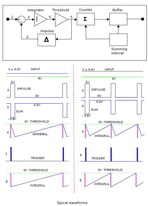
For the purpose of introduction, Figure 1 illustrates the concept of voltage-to-frequency conversion, in an unclocked form that resembles delta-sigma modulation, and is called asynchronous modulation[2], asynchronous delta-sigma modulation,[3][4] or free-running modulators.[5]
Shown below that are waveforms at points designated by numbers 1 to 5 for an input of 0.2 volts in the left column and 0.4 volts in the right column. The stream of delta impulses generated at each threshold crossing is shown at (2) and the difference between (1) and (2) is shown at (3). This difference is integrated to produce the waveform (4). The threshold detector generates a pulse (5) which starts as the waveform (4) crosses the threshold and is sustained until the waveform (4) falls below the threshold. The threshold (5) triggers the impulse generator to produce a fixed-strength impulse.
The integral (4) crosses the threshold in half the time in the right column than in the left column. Thus the frequency of impulses is doubled. Hence the count increments at twice the speed on the right to that on the left; this pulse rate doubling is consistent with the input voltage being doubled.
Construction of the waveforms illustrated at (4) is aided by concepts associated with the Dirac delta function in that, by definition, all impulses of the same strength produce the same step when integrated. Then (4) is constructed using an intermediate step (6), a hypothetical waveform not in the circuit but in which each integrated ideal delta function impulse is integrated to a step. The effect of the finite duration of the actual pulse is constructed in (4) by drawing a line from the base of the impulse step at zero volts to intersect the decay line from (6) at the full duration of the pulse.
In the circuit outside the loop, the summing interval is a predetermined fixed time, and at its expiry the count is stored, and the buffer and the counter are reset. The buffer then presents a sequence of digital values corresponding to quantizations of the analog signal levels during the summing intervals. Using a summing interval is a way (not necessarily the ideal way) to quantize the asynchronous pulse stream to a code; it will have less quantization error if the interval start is synchronized to a pulse.
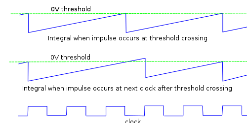
Delta-sigma converters further constrain operation of the impulse generator such that the start of the impulse is delayed until the next occurrence of the appropriate clock-pulse boundary. The effect of this delay is illustrated in Figure 1a for a sequence of impulses which occur at a nominal 2.5 clock intervals.
Practical implementation
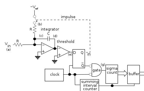
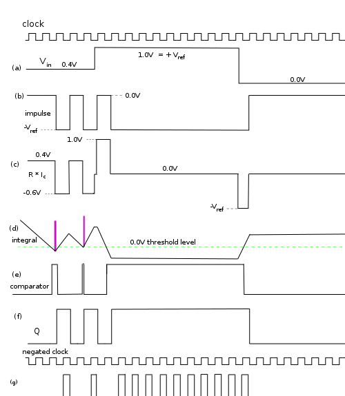
A circuit diagram for a delta-sigma modulator implementation is shown in Figure 1b, with the associated waveforms in Figure 1c. The waveforms shown in Figure 1c are unusually complicated because they are intended to illustrate the loop behaviour under extreme conditions, Vin saturated at full scale of 1.0 V, and saturated at zero. An intermediate state is also indicated, Vin at 0.4V, where it is very similar to the operation of the illustration of Figure 1.
From the top of Figure 1c, the waveforms, labelled as they are on the circuit diagram, are:
- The clock
- (a) Vin – this is shown as varying from 0.4 V initially to 1.0 V and then to zero volts to show the effect on the feedback loop.
- (b) The impulse waveform feeding the integrator. Controlled by flip-flop output (f) below.
- (c) The current into the capacitor, Ic, is the linear sum of the impulse reference voltage divided by R and Vin divided by R. To show this sum as a voltage the product R × Ic is plotted. The input impedance of the amplifier is regarded as so high that the current drawn by the input is neglected. The capacitor is connected between the negative input terminal of the amplifier and its output terminal. With this connection it provides a negative feedback path around the amplifier. The input voltage change is equal to the output voltage change divided by the amplifier gain. With very high amplifier gain the change in input voltage can be neglected and so the input voltage is held close to the voltage on the positive input terminal which in this case is held at 0V. Because the voltage at the input terminal is 0V the voltage across R is simply Vin so that the current into the capacitor is the input voltage divided by the resistance of R.
- (d) The negated integral of Ic. This negation is standard for the op amp integrator and comes about because the current into the capacitor at the amplifier input is the current out of the capacitor at the amplifier output and the voltage is the integral of the current divided by the capacitance C.
- (e) The comparator output. The comparator is a very high gain amplifier with its plus input terminal connected for reference to 0.0 V. Whenever the negative input terminal is taken negative with respect the positive terminal of the amplifier the output saturates positive and conversely negative saturation for positive input. Thus the output saturates positive whenever the integral (d) goes below the 0 V reference level and the output remains there until (d) goes positive with respect to the 0 V reference.
- (f) The impulse timer is a D-type positive-edge-triggered flip-flop. Input information applied at D is transferred to Q on the occurrence of the positive edge of the clock pulse. Thus when the comparator output (e) is positive, Q goes positive or remains positive at the next positive clock edge. Similarly, when (e) is negative, Q goes negative at the next positive clock edge. Q controls the electronic switch to generate the current impulse (b) into the integrator. Examination of the waveform (e) during the initial period illustrated, when Vin is 0.4 V, shows (e) crossing the threshold well before the positive edge of the clock pulse so that there is an appreciable delay before the impulse starts. After the start of the impulse there is further delay while (d) climbs back past the threshold. During this time the comparator output (e) remains high but goes low before the next trigger edge at which point the impulse timer goes low to follow the comparator. Thus the clock, in part, determines the duration of the impulse. For the next impulse the threshold is crossed immediately before the trigger edge and so the comparator is only briefly positive. Vin (a) then goes to full scale, +Vref, shortly before the end of the next impulse. For the remainder of that impulse the capacitor current (c) goes to zero and hence the integrator slope briefly goes to zero. Following this impulse, the full-scale positive current flows (c) and the integrator sinks at its maximum rate and so crosses the threshold well before the next trigger edge. At that edge the impulse starts and the Vin current is now matched by the reference current so that the net capacitor current (c) is zero. The integration now has zero slope and remains at the negative value it had at the start of the impulse. This has the effect that the impulse current remains switched on because Q is stuck positive because the comparator is stuck positive at every trigger edge. This is consistent with contiguous, butting impulses which is representative of full-scale input. Next Vin (a) goes to zero which causes the current sum (c) to go fully negative and the integral ramps up. It shortly thereafter crosses the threshold and this in turn is followed by Q, thus switching the impulse current off. The capacitor current (c) is now zero and so the integral slope is zero, remaining constant at the value it had acquired at the end of the impulse.
- (g) The countstream is generated by gating the negated clock with Q to produce this waveform. Thereafter the summing interval, sigma count, and buffered count are produced using appropriate counters and registers.
Improvements to resolution and noise
Examination of Figure 1c(g) shows that there are zero pulses in the countstream when the input voltage is zero. This condition can have the effect that high-frequency components of a complex signal are not resolved. This effect is known as intermodulation distortion (IMD). One of the pitfalls of applying linear analysis to a nonlinear system is that IMD, because it can be a consequence of nonlinearity, is not present in the analysis. Purely for illustrative purposes, a method to mitigate this would be to add an 0.5 volt constant bias to the input voltage so the it now can swing +/− 0.5 V about the bias. This now has zero pulses in the countstream when the input is −0.5 V. Then we must limit the input swing to +/− 0.4 V, say, so that the minimum countstream frequency is greater than zero. We can choose the clock frequency so that the minimum countstream frequency at −0.4 V is much greater than the Nyquist rate, so that even the highest input frequency component is resolved. We can increase the clock frequency still higher until a lowpass filter sufficiently removes the pulsations while fully recovering the input signal. In this illustrative discussion the filtered signal will also recover the bias which can be removed by an analogue adder, while still retaining the DC component of the input signal.
Remarks
According to Wooley,[6] the seminal paper combining feedback with oversampling to achieve delta modulation was by F. de Jager in 1952.[7]
The delta-sigma configuration was devised by Inose et al. in 1962 to solve problems in the accurate transmission of analog signals.[8] In that application it was the pulse stream that was transmitted and the original analog signal recovered with a lowpass filter after the received pulses had been reformed. This low pass filter performed the summation function associated with Σ. The highly mathematical treatment of transmission errors was introduced by them and is appropriate when applied to the pulse stream but these errors are lost in the accumulation process associated with Σ.
For the analogue to digital conversion application each pulse in the count stream is a sample of the mean of the input voltage equal to the reference voltage divided the interval between pulses, ts. This because it is an integration of the input waveform over interval ts. Frequency domain analysis of the complex waveform in this interval, ts, will represent it by the sum of a constant plus a fundamental and harmonics each of which has an exact integer number of cycles over ts. The integral of a sine wave over one or more full cycles is zero. Therefore, the integral of the incoming waveform over the interval ts reduces to the mean over the interval. The count, N, accumulated during the summing interval represents N samples of the mean and N divided by the count defining the summing interval is thus the mean of means and so subject to little variance.
Digital to analogue conversion
In general, a DAC converts a digital number, N, representing some analogue value into that analogue voltage value. To make the conversion the digital number is first loaded into a counter. Then the counter is counted down to zero with a string of pulses equal in number to N. Each pulse of the string is given a known integral, δ. Then the string is integrated to produce N.δ, the sum of the pulses. This is the required analogue voltage.
In some applications where an analogue signal is represented by a series of digital numbers that require conversion to a frequency modulated stream it may be sufficient to take the stream of pulses (two or three level) resulting from the DAC conversion of each number N in turn and apply that stream through a low pass filter directly to the output. The output before filtering will be a crudely frequency modulated stream with bursts of pulses proportional in length and number to the analogue of N separated by blank intervals between bursts.
In order to remove the blank intervals and improve the noise performance the full conversion to analogue voltage of each successive N by the DAC described above may be held in a sample and hold circuit then passed to a delta sigma converter to produce a stream of contiguous bursts each of which has its frequency proportional to its generating N.
Decimation structures
The conceptually simplest decimation structure is a counter that is reset to zero at the beginning of each integration period, then read out at the end of the integration period.
The multi-stage noise shaping (MASH)[9] structure has a noise shaping property, and is commonly used in digital audio and fractional-N frequency synthesizers. It comprises two or more cascaded overflowing accumulators, each of which is equivalent to a first-order sigma-delta modulator. The carry outputs are combined through summations and delays to produce a binary output, the width of which depends on the number of stages (order) of the MASH. Besides its noise shaping function, it has two more attractive properties:
- simple to implement in hardware; only common digital blocks such as accumulators, adders, and D flip-flops are required
- unconditionally stable (there are no feedback loops outside the accumulators)
A very popular decimation structure is the sinc filter. For second-order modulators, the sinc3 filter is close to optimum.[10][11]
Example of decimation
Let's have, for instance, an 8:1 decimation filter and a 1-bit bitstream; if we have an input stream like 10010110, counting the number of ones, we get 4. Then the decimation result is 4/8 = 0.5. We can then represent it with a 3-bits number 100 (binary), which means half of the largest possible number. In other words,
- the sample frequency is reduced by a factor of eight
- the serial (1-bit) input bus becomes a parallel (3-bits) output bus.
Once decimation is applied and if the n bit codes are transmitted the signal becomes pulse code modulation. Decimation is strongly associated with delta sigma modulation but the distinction needs to be made.
Variations
There are many kinds of ADC that use this delta-sigma structure. The above analysis focuses on the simplest 1st-order, 2-level, uniform-decimation sigma-delta ADC. Many ADCs use a second-order 5-level sinc3 sigma-delta structure. Much of what follows uses an arcane shorthand using symbols representing operational functions with analysis given in terms of Laplace transforms, etc. This is the lingua franca of the data transmission industry and it does not communicate to the general public. If a fuller documentation of a particular method is needed look no further than the patents. (Patent examiners generally require full disclosure.) An excellent history is "The Evolution of Oversampling Analog-to-Digital Converters" by Bruce A. Wooley which gives many references to the relevant patents.
Second-order and higher-order modulator

The number of integrators, and consequently, the numbers of feedback loops, indicates the order of a ΔΣ modulator; a second-order ΔΣ modulator is shown in Figure 4. First-order modulators are unconditionally stable, but stability analysis must be performed for higher-order modulators.
3-level and higher quantizer
The modulator can also be classified by the number of bits it has in its output, which strictly depends on the output of the quantizer. The quantizer can be realized with a N-level comparator, thus the modulator has log2N-bit output. A simple comparator has 2 levels and so is 1 bit quantizer; a 3-level quantizer is called a "1.5" bit quantizer; a 4-level quantizer is a 2 bit quantizer; a 5-level quantizer is called a "2.5 bit" quantizer.[12]
Relationship to delta modulation
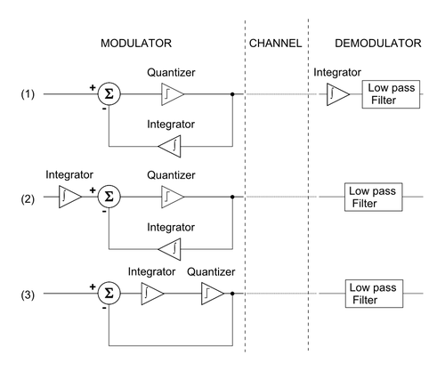

Delta-sigma modulation is inspired by delta modulation, as shown in Figure 2. If quantization were homogeneous (e.g., if it were linear), the following would be a sufficient derivation of the equivalence:
- Start with a block diagram of a delta modulator/demodulator.
- The linearity property of integration, , makes it possible to move the integrator, which reconstructs the analog signal in the demodulator section, in front of the delta modulator.
- Again, the linearity property of the integration allows the two integrators to be combined and a delta-sigma modulator/demodulator block diagram is obtained.
Because the quantizer is not homogeneous, delta-sigma is inspired by delta modulation, but the two are distinct in operation.
From the first block diagram in Figure 2, the integrator in the feedback path can be removed if the feedback is taken directly from the input of the low-pass filter. Hence, for delta modulation of input signal u, the low-pass filter sees the signal
However, sigma-delta modulation of the same input signal places at the low-pass filter
In other words, delta-sigma and delta modulation swap the position of the integrator and quantizer. The net effect is a simpler implementation that has the added benefit of shaping the quantization noise away from signals of interest (i.e., signals of interest are low-pass filtered while quantization noise is high-pass filtered). This effect becomes more dramatic with increased oversampling, which allows for quantization noise to be somewhat programmable. On the other hand, delta modulation shapes both noise and signal equally.
Additionally, the quantizer (e.g., comparator) used in delta modulation has a small output representing a small step up and down the quantized approximation of the input while the quantizer used in delta-sigma must take values outside of the range of the input signal, as shown in Figure 3.
In general, delta-sigma has some advantages versus delta modulation:
- The structure is simplified as
- only one integrator is needed,
- the demodulator can be a simple linear filter (e.g., RC or LC filter) to reconstruct the signal and
- the quantizer (e.g., comparator) can have full-scale outputs
- The quantized value is the integral of the difference signal, which makes it less sensitive to the rate of change of the signal.
Quantization theory formulas
When a signal is quantized, the resulting signal has approximately the second-order statistics of a signal with independent white noise added. Assuming that the signal value is in the range of one step of the quantized value with an equal distribution, the root mean square value of this quantization noise is
In reality, the quantization noise is, of course, not independent of the signal and this dependence results in limit cycles and is the source of idle tones and pattern noise in sigma-delta converters.
Quantization noise may be reduced by increasing the oversampling ratio (OSR) defined by
where is the sampling frequency and is Nyquist rate.
The RMS noise voltage within the band of interest () can be expressed in terms of OSR
Oversampling
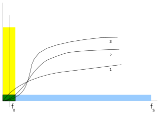
ΔΣ modulation is a technique of oversampling to reduce the noise in the band of interest (green in Figure 5), which avoids the use of high-precision analog circuits for the anti-aliasing filter. The total quantization noise is the same both in a Nyquist converter (in yellow) and in an oversampling converter (in blue), but it is distributed over a different spectrum. In ΔΣ converters, noise is further reduced at low frequencies, which is the band where the signal of interest is, and it is increased at the higher frequencies, where it can be filtered out. This technique is known as noise shaping.
For a first-order delta-sigma modulator, the noise is shaped by a filter with transfer function Hn(z) = [1 − z−1]. Assuming that the sampling frequency fs is large compared to a signal frequency of interest, f0, the quantization noise in the desired signal bandwidth can be approximated as:
- .
Similarly for a second-order delta-sigma modulator, the noise is shaped by a filter with transfer function Hn(z) = [1 − z−1]2. The in-band quantization noise can be approximated as:
- .
In general, for a N-order ΔΣ modulator, the variance of the in-band quantization noise is:
- .
When the sampling frequency is doubled, the signal-to-quantization-noise ratio is improved by 6N + 3 dB for a N-order ΔΣ modulator. The higher the oversampling ratio, the higher the signal-to-noise ratio and the higher the resolution in bits.
Another key aspect given by oversampling is the speed/resolution tradeoff. The decimation filter put after the modulator not only filters the whole sampled signal in the band of interest (cutting the noise at higher frequencies), but also reduces the frequency of the signal, increasing its resolution. This is obtained by a sort of averaging of the higher-data-rate bitstream.
Naming
The technique was first presented in the early 1960s by professor Yasuhiko Yasuda while he was a student at the University of Tokyo.[13][14] The name delta-sigma comes directly from the presence of a delta modulator and an integrator, as firstly introduced by Inose et al. in their patent application.[8] That is, the name comes from integrating or summing differences, which, in mathematics, are operations usually associated with Greek letters sigma and delta respectively. Both names sigma-delta and delta-sigma are frequently used.
References
- Sangil Park, Principles of Sigma-Delta Modulation for Analog-to-Digital Converters (PDF), Motorola, retrieved 2017-09-01
- J. Candy and O. Benjamin (September 1981). "The Structure of Quantization Noise from Sigma-Delta Modulation". IEEE Transactions on Communications. 29 (9): 1316–1323. doi:10.1109/TCOM.1981.1095151.CS1 maint: uses authors parameter (link)
- Kikkert, C. J., and D. J. Miller (1975). "Asynchronous delta sigma modulation". Proceedings of the Institution of Radio and Electronics Engineers. 36: 83–88. Retrieved 19 February 2019.CS1 maint: multiple names: authors list (link)
- Gaggl, Richard (2012). Delta-Sigma A/D-Converters. Springer. pp. 41–45. ISBN 9783642345432. Retrieved 19 February 2019.
- Micheal A.P. Pertijs and Johan Huijsing (2006). Precision Temperature Sensors in CMOS Technology. Springer. pp. 111–113. ISBN 9781402052583.CS1 maint: uses authors parameter (link)
- "The Evolution of Oversampling Analog-to-Digital Converters" Bruce A. Wooley
- "Deltamodulation, a method of P.C.M. transmission using the 1-unit code" F. de Jager
- H. Inose, Y. Yasuda, J. Murakami, "A Telemetering System by Code Manipulation – ΔΣ Modulation", IRE Trans on Space Electronics and Telemetry, Sep. 1962, pp. 204-209.
- "15-25 MHZ Fractional-N Synthesizer".
- A Novel Architecture for DAQ in Multi-channel, Large Volume, Long Drift Liquid Argon TPC by S. Centro, G. Meng, F. Pietropaola, S. Ventura 2006
- Lombardi, A.; Bonizzoni, E.; Malcovati, P.; Maloberti, F. (2007). "A Low Power Sinc3 Filter for ΣΔ Modulators". 2007 IEEE International Symposium on Circuits and Systems. pp. 4008–4011. doi:10.1109/ISCAS.2007.378797. ISBN 978-1-4244-0920-4.
- Sigma-delta class-D amplifier and control method for a sigma-delta class-D amplifier by Jwin-Yen Guo and Teng-Hung Chang
- 発見と発明のデジタル博物館卓越研究データベース・電気・情報通信関連・研究情報(登録番号671)
- Sangil Park, Principles of sigma-delta modulation for analog-to-digital converters (PDF), Motorola, archived from the original (PDF) on 2006-06-21
- Walt Kester (October 2008). "ADC Architectures III: Sigma-Delta ADC Basics" (PDF). Analog Devices. Retrieved 2010-11-02.
- R. Jacob Baker (2009). CMOS Mixed-Signal Circuit Design (2nd ed.). Wiley-IEEE. ISBN 978-0-470-29026-2.
- R. Schreier; G. Temes (2005). Understanding Delta-Sigma Data Converters. ISBN 978-0-471-46585-0.
- S. Norsworthy; R. Schreier; G. Temes (1997). Delta-Sigma Data Converters. ISBN 978-0-7803-1045-2.
- J. Candy; G. Temes (1992). Oversampling Delta-sigma Data Converters. ISBN 978-0-87942-285-1.
External links
- 1-bit A/D and D/A Converters
- Sigma-delta techniques extend DAC resolution article by Tim Wescott 2004-06-23
- Tutorial on Designing Delta-Sigma Modulators: Part I and Part II by Mingliang (Michael) Liu
- Gabor Temes' Publications
- Sigma-Delta Modulation Primer Part II Contains Block diagrams, code, and simple explanations
- Example Simulink model & scripts for continuous-time sigma-delta ADC Contains example matlab code and Simulink model
- Bruce Wooley's Delta-Sigma Converter Projects
- An Introduction to Delta Sigma Converters (which covers both ADCs and DACs sigma-delta)
- Demystifying Sigma-Delta ADCs. This in-depth article covers the theory behind a Delta-Sigma analog-to-digital converter.
- One-Bit Delta Sigma D/A Conversion Part I: Theory article by Randy Yates presented at the 2004 comp.dsp conference
- MASH (Multi-stAge noise SHaping) structure with both theory and a block-level implementation of a MASH
- Continuous time sigma-delta ADC noise shaping filter circuit architectures discusses architectural trade-offs for continuous-time sigma-delta noise-shaping filters
- Delta Sigma Converters: Modulation – intuitive motivation for why a delta-sigma modulator works
- Digital accelerometer with feedback control using sigma-delta modulation