Zener effect
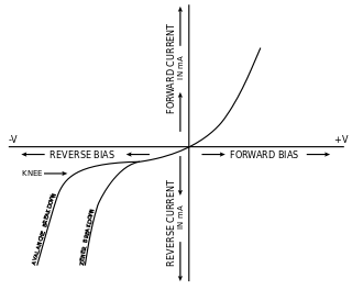
In electronics, the Zener effect (employed most notably in the appropriately named Zener diode) is a type of electrical breakdown, discovered by Clarence Melvin Zener. It occurs in a reverse biased p-n diode when the electric field enables tunneling of electrons from the valence to the conduction band of a semiconductor, leading to numerous free minority carriers which suddenly increase the reverse current.[1]

Mechanism
Under a high reverse-bias voltage, the p-n junction's depletion region widens which leads to a high-strength electric field across the junction.[2] Sufficiently strong electric fields enable tunneling of electrons across the depletion region of a semiconductor, leading to numerous free charge carriers. This sudden generation of carriers rapidly increases the reverse current and gives rise to the high slope conductance of the Zener diode.
Relationship to the avalanche effect
The Zener effect is distinct from avalanche breakdown. Avalanche breakdown involves minority carrier electrons in the transition region being accelerated, by the electric field, to energies sufficient for freeing electron-hole pairs via collisions with bound electrons. The Zener and the avalanche effect may occur simultaneously or independently of one another. In general, diode junction breakdowns occurring below 5 volts are caused by the Zener effect, whereas breakdowns occurring above 5 volts are caused by the avalanche effect. Breakdowns occurring at voltages close to 5V are usually caused by some combination of the two effects. Zener breakdown voltage is found to occur at electric field intensity of about 3×10⁷ V/m.[1] Zener breakdown occurs in heavily doped junctions (p-type semiconductor moderately doped and n-type heavily doped), which produces a narrow depletion region.[2] The avalanche breakdown occurs in lightly doped junctions, which produce a wider depletion region. Temperature increase in the junction increases the contribution of the Zener effect to breakdown, and decreases the contribution of the avalanche effect.
References
- "PN junction breakdown characteristics". Circuits Today. August 25, 2009. Retrieved August 16, 2011.
- "Zener and Avalanche Breakdown/Diodes", School of Engineering and Applied Sciences, Harvard University