Voodoo 5
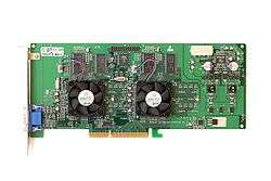
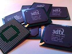
The Voodoo 5 was the last and most powerful graphics card line that 3dfx Interactive released. All members of the family were based upon the VSA-100 graphics processor.[1] Only the single-chip Voodoo 4 4500 and dual-chip Voodoo 5 5500 made it to market.

Architecture and performance

The VSA-100 graphics chip is a direct descendant of "Avenger", more commonly known as Voodoo3. It was built on a 250 nm semiconductor manufacturing process, as with Voodoo3. However, the process was tweaked with a 6th metal layer to allow for better density and speed, and the transistors have a slightly shorter gate length and thinner gate oxide. VSA-100 has a transistor count of roughly 14 million, compared to Voodoo3's ~8 million. The chip has a larger texture cache than its predecessors and the data paths are 32 bits wide rather than 16-bit. Rendering calculations are 40 bits wide in VSA-100 but the operands and results are stored as 32-bit.[2]
One of the design goals for the VSA-100 was scalability. The name of the chip is an abbreviation for "Voodoo Scalable Architecture." By using one or more VSA-100 chips on a board, the various market segments for graphics cards are satisfied with just a single graphics chip design. Theoretically, anywhere from 1 to 32 VSA-100 GPUs could be run in parallel on a single graphics card, and the fillrate of the card would increase proportionally. On cards with more than one VSA-100, the chips are linked using 3dfx's Scan-Line Interleave (SLI) technology. A major drawback to this method of performance scaling is that various parts of hardware are needlessly duplicated on the cards and board complexity increases with each additional processor.
3dfx changed the rendering pipeline from one pixel pipeline with twin texture mapping units (Voodoo2/3) to a dual pixel pipeline design with one texture mapping unit on each.[3] This design, commonly referred to as a 2x1 configuration, has an advantage over the prior 1x2 design with the ability to always output 2 pixels and 2 texels per clock instead of 1 pixel and 2 texels per clock.
This is the first 3dfx graphics chip to support full 32-bit color depth in 3D, compared to 16-bit color depth with all previous designs. The limitation of 256px x 256px maximum texture dimensions was also addressed and VSA-100 can use up to 2048px x 2048px textures. Additionally, 3dfx implemented the FXT1 and DXTC texture compression techniques.[3]
The VSA-100 supports a hardware accumulation buffer, known as the "T-buffer". When rendering to the T-buffer, VSA-100 can store the combined outputs of several frames. This mechanism allows for creation of effects such as motion blur (if used temporally) and anti-aliasing (if used spatially).[3] VSA-100 supports rotated-grid super-sampling anti-aliasing (RGSS AA) modes, with a maximum anti-aliasing level determined by the number of VSA-100 chips in the SLI configuration. One chip allows 2X AA, two chips allows 4X AA, four chips provides for 8X AA and so on. The RGSS method of anti-aliasing combines multiple samples of each frame, resulting in higher quality than the brute force ordered-grid over-sampling of ImgTech PowerVR, ATI Radeon DDR and NVIDIA GeForce 2.[4]
The chip implements a 128-bit SDRAM interface, again similar to the Voodoo3. Memory capacity and bandwidth is separately dedicated to each VSA-100 processor. While capacity is not cumulative across the entire card, bandwidth is effectively cumulative and thus a card with 2x VSA-100 processors has similar bandwidth to a single-chip graphics card using 128-bit DDR memory. Memory is clocked synchronously with the VSA-100 chip. Later, unreleased boards were planned to offer a 64-bit DDR memory design instead, in order to reduce board costs through lower complexity, while offering similar RAM performance.
While VSA-100 is an AGP 4x capable graphics processor, 3dfx did not implement AGP texturing.
Models
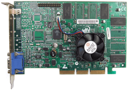
Voodoo 4 4500

Released after the Voodoo 5 5500, the Voodoo4 4500 is the budget implementation of the VSA-100 product. It used only one VSA-100 chip and did not need an additional power connection. It was more expensive yet it was beaten in almost all areas by the GeForce2 MX and Radeon SDR.[5]
Voodoo 5 5000
The unreleased Voodoo 5 5000 was to be similar to the 5500 but with half of the RAM capacity (32 MB total).
Voodoo 5 5500
The Voodoo 5 5500 comes in three flavors: a universal AGP version (AGP 1/2x, prototypes were made with AGP4x-interface) with full sideband support, PCI, and the Mac Edition, which is only available for PCI, though could run in 66 MHz PCI slots. The Mac Edition has dual link DVI-D and VGA-A outputs, the other versions just have one VGA-out.
In games, the Voodoo 5 5500 is able to outperform the NVIDIA GeForce 256 and ATI Rage 128 MAXX, but unfortunately Voodoo5 5500 was late to market and was up against the new GeForce 2 GTS and Radeon DDR, both of which easily outperformed the Voodoo 5.[6]
Voodoo 5 6000
The Voodoo 5 6000 is the unreleased high-end product in the Voodoo5 line. It was to use four 166 MHz VSA-100 processors, each with its own 32 MB of 166 MHz SDRAM, resulting in the first 128 MB graphics card (consisting of sixteen 8 MB chips). Approximately 1000+ test cards were produced. Because the card used more power than the AGP specification allowed for, a special power supply called Voodoo Volts had to be included with it. This would have been an external device that would connect to an AC outlet. Most of the prototype cards utilized a standard internal power supply molex power connector.
With regards to performance, little was known until enthusiasts were able to get pre-release hardware and run tests on it. The results showed that the Voodoo 5 6000 outperformed the GeForce 2 Ultra and Radeon 7500, which were the fastest iterations of the GeForce 2 and Radeon R100 lines, respectively. (It was rumored that GeForce 2 Ultra was intended to prevent 3dfx taking the lead with their Voodoo 5 6000.) In some cases, the 6000 was shown to compete well with the next-generation GeForce 3.[7]
Unfortunately the production cost of the Voodoo5 6000 would have likely hampered its competitiveness from a profitability standpoint. Compared to the single-chip GeForce and Radeon cards, a Voodoo5 6000 is burdened with much redundancy and a complicated board. It was projected to have a US$600 price tag, considerably higher than competing parts. Despite its high price point, the Voodoo5 6000 would not have offered next-generation DirectX 8.0 vertex and pixel shaders that would be found in the GeForce 3 (which was intended by Nvidia to replace the short-lived GeForce 2 Ultra as its flagship product) and Radeon 8500, nor even DirectX 7 features such as hardware transform and lighting acceleration for vertices. The precarious financial situation of 3dfx was another factor contributing to the 6000's demise.
There were five revisions of the Voodoo 5 6000: (the numbers after the model state the build week: 10 for week 10, 00 for year 2000).
Intel Revision 1 (model 1000-1900)
This was an early alpha of the card primarily used for photos and testing purposes. These cards generally had a short life expectancy, and were largely incompatible with various motherboards at the time. They also typically could not achieve speeds above 143 MHz without suffering from VSA-100 "death". This revision used an Intel PCI bridge chip, was equipped with 128 MB of 5.4ns SDRAM and used a proprietary external 3dfx power supply. Initial models had the chips mounted in the arrangement seen in the photograph, but this required a PCB with eight circuitry layers (most GeForce 2 cards were four-layer, while the Voodoo 5 5500 was six-layer) and would have been unreasonably expensive. All of the later revisions had the four chips mounted in a row.
HiNT Revision 2 (model 2000-2900)
This version dropped the Intel PCI bridge chip in favor of a HiNT bridge chip. These cards were able to be powered by either the internal system PSU or by a proprietary 3dfx external power supply, a feature seen in all subsequent prototype revisions. The clock speed varied from card to card, generally either 166 or 183 MHz. The VSA-100 chips used still did not have a long life expectancy, and may have had problems running anti-aliasing. This revision had 128 MB of 5.0ns SDRAM.
HiNT Revision 3 (model 3000-3500)
Cards from this revision varied in stability from dead to fully functional. A lot of problems had been fixed in this revision, but it still had VSA-100 thermal death problems above 183 MHz. These cards either had 166 or 183 MHz VSA-100 GPUs.
HiNT Revision 4 (3600-3700)
3dfx decided on 166 MHz due to issues with the 6000 running properly at 183 MHz due to a design flaw with the PCB. Most of the problems seen in earlier revisions were fixed, although there may have been glitches while in anti-aliasing mode on some cards. Most of the known cards are revision A from week 37, 2000.
HiNT Revision 5 (model 3900)
Little is known about this series except that this is the final revision. It was meant to be the retail unit, but shortly after the run of 10 were produced, the 6000 series was cancelled.
List
| Model | Launch | Code name | Fab (nm) | Bus interface | Memory (MiB) | Core clock (MHz) | Memory clock (MHz) | Core config1 | Fillrate | Memory | Direct3D support | |||||
|---|---|---|---|---|---|---|---|---|---|---|---|---|---|---|---|---|
| MOperations/s | MPixels/s | MTexels/s | MVertices/s | Bandwidth (GB/s) | Bus type | Bus width (bit) | ||||||||||
| Voodoo4 4000 | Never released | VSA-100 | 250 | AGP 4x, PCI | 16 | 166 | 166 | 2:2 | 332 | 332 | 332 | 0 | 2.656 | SDR | 128 | 6.0 |
| Voodoo4-2 4000 | Never released | VSA-101 | 180 | AGP | 16 | ? | ? | 2:2 | ? | ? | ? | 0 | ? | SDR | 128 | 6.0 |
| Voodoo4-2 4200 | Never released | VSA-101 | 180 | AGP, PCI | 16, 32 | 143 | 143 | 2:2 | 143 | 143 | ? | 0 | ? | DDR | 64 | 6.0 |
| Voodoo4-2 4200 | Never released | VSA-101 | 180 | PCI | 32 | 166 | 166 | 2:2 | 166 | 166 | ? | 0 | ? | DDR | 64 | 6.0 |
| Voodoo4 4500 | October 13, 2000 | VSA-100 | 250 | AGP 2x[8]/4x,[8] PCI | 32 | 166 | 166 | 2:2 | 332 | 332 | 332 | 0 | 2.656 | SDR | 128 | 6.0 |
| Voodoo4 4800 | Never released | VSA-100 | 250 | AGP 4x, PCI | 64 | 166 | 166 | 2:2 | 333 | 333 | 333 | 0 | 2.656 | SDR | 128 | 6.0 |
| Voodoo5 5000 | Never released | VSA-100 x2 | 250 | AGP 4x, PCI | 32 | 166 | 166 | 2:2 x2 | 664 | 664 | 664 | 0 | 2.656 | SDR | 128 | 6.0 |
| Voodoo5 5500 | June 22, 2000 | VSA-100 x2 | 250 | AGP 2x,[8] PCI | 64 | 166 | 166 | 2:2 x2 | 664 | 664 | 664 | 0 | 5.33 | SDR | 128 | 6.0 |
| Voodoo5 6000 | Never released | VSA-100 x4 | 250 | AGP 4x, PCI | 128 | 166 | 166 | 2:2 x4 | 1328 | 1328 | 1328 | 0 | 10.66 | SDR | 256 | 6.0 |
Successor
The successor to the Voodoo 5 series, codenamed "Rampage", was already planned and had been in development for years. It was supposed to have a smaller semiconductor process, support for DDR SDRAM, 200+ MHz core, and a T&L unit. However, it was early in its development and only approximately twenty working cards were produced before 3dfx went bankrupt, and most assets were purchased by NVIDIA in late 2000.[9][10]
Competing chipsets
- ATI Rage 128 MAXX and Radeon
- NVIDIA GeForce 256 and GeForce2
- PowerVR Series 3 (Kyro and Kyro II)
- S3 Savage 2000
- Matrox Millennium G400 MAX
References
- Lal Shimpi, Anand. 3dfx Voodoo5 5500, Anandtech, July 11, 2000.
- 3dfx Interview with Peter Wicher, Hot Hardware, December 15, 2001.
- 3dfx Voodoo 5 5500 Preview, Firing Squad, April 24, 2000.
- Multi-Sampling Anti-Aliasing Explained, Firing Squad, February 13, 2001.
- AnandTech - 3dfx Voodoo4 4500AGP
- Guido Shah, Sarju. Voodoo5 5500 Review, Firingsquad, 2000-07-14.
- Jasper. 3dfx Voodoo 5 6000 Review Archived 2006-08-22 at the Wayback Machine, Sudhian, July 26, 2006.
- "Identify your 3dfx Hardware with Part No. and/or special Markings". FalconFly Central. Archived from the original on June 7, 2004.
- TDG-3dfx-Rampage
- Support for 3dfx Voodoo cards
External links
- FalconFly.de 3dfx Archive - home of the 3dfx software and driver archive. Many enhanced 3rd party drivers for all generations of Voodoos.
- 3dfxZone.it - source of hardware information and software for 3dfx video cards.