Vapor–liquid–solid method
The vapor–liquid–solid method (VLS) is a mechanism for the growth of one-dimensional structures, such as nanowires, from chemical vapor deposition. The growth of a crystal through direct adsorption of a gas phase on to a solid surface is generally very slow. The VLS mechanism circumvents this by introducing a catalytic liquid alloy phase which can rapidly adsorb a vapor to supersaturation levels, and from which crystal growth can subsequently occur from nucleated seeds at the liquid–solid interface. The physical characteristics of nanowires grown in this manner depend, in a controllable way, upon the size and physical properties of the liquid alloy.
Historical background
The VLS mechanism was proposed in 1964 as an explanation for silicon whisker growth from the gas phase in the presence of a liquid gold droplet placed upon a silicon substrate.[1] The explanation was motivated by the absence of axial screw dislocations in the whiskers (which in themselves are a growth mechanism), the requirement of the gold droplet for growth, and the presence of the droplet at the tip of the whisker during the entire growth process.
Introduction
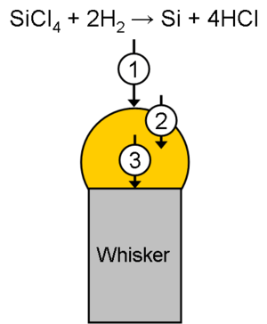
The VLS mechanism is typically described in three stages:[2]
- Preparation of a liquid alloy droplet upon the substrate from which a wire is to be grown
- Introduction of the substance to be grown as a vapor, which adsorbs on to the liquid surface, and diffuses into the droplet
- Supersaturation and nucleation at the liquid/solid interface leading to axial crystal growth
Experimental technique
The VLS process takes place as follows:
- A thin (~1–10 nm) Au film is deposited onto a silicon (Si) wafer substrate by sputter deposition or thermal evaporation.
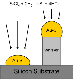
- The wafer is annealed at temperatures higher than the Au-Si eutectic point, creating Au-Si alloy droplets on the wafer surface (the thicker the Au film, the larger the droplets). Mixing Au with Si greatly reduces the melting temperature of the alloy as compared to the alloy constituents. The melting temperature of the Au:Si alloy reaches a minimum (~363 °C) when the ratio of its constituents is 4:1 Au:Si, also known as the Au:Si eutectic point.
- Lithography techniques can also be used to controllably manipulate the diameter and position of the droplets (and as you will see below, the resultant nanowires).
- One-dimensional crystalline nanowires are then grown by a liquid metal-alloy droplet-catalyzed chemical or physical vapor deposition process, which takes place in a vacuum deposition system. Au-Si droplets on the surface of the substrate act to lower the activation energy of normal vapor-solid growth. For example, Si can be deposited by means of a SiCl4:H2 gaseous mixture reaction (chemical vapor deposition), only at temperatures above 800 °C, in normal vapor-solid growth. Moreover, below this temperature almost no Si is deposited on the growth surface. However, Au particles can form Au-Si eutectic droplets at temperatures above 363 °C and adsorb Si from the vapor state (because Au can form a solid-solution with all Si concentrations up to 100%) until reaching a supersaturated state of Si in Au. Furthermore, nanosized Au-Si droplets have much lower melting points (ref) because the surface area-to-volume ratio is increasing, becoming energetically unfavorable, and nanometer-sized particles act to minimize their surface energy by forming droplets (spheres or half-spheres).
- Si has a much higher melting point (~1414 °C) than that of the eutectic alloy, therefore Si atoms precipitate out of the supersaturated liquid-alloy droplet at the liquid-alloy/solid-Si interface, and the droplet rises from the surface. This process is illustrated in figure 1.
Typical features of the VLS method
- Greatly lowered reaction energy compared to normal vapor-solid growth.
- Wires grow only in the areas activated by the metal catalysts and the size and position of the wires are determined by that of the metal catalysts.
- This growth mechanism can also produce highly anisotropic nanowire arrays from a variety of material.
Requirements for catalyst particles
The requirements for catalysts are:[3]
- It must form a liquid solution with the crystalline material to be grown at the nanowire growth temperature.
- The solid solubility of the catalyzing agent is low in the solid and liquid phases of the substrate material.
- The equilibrium vapor pressure of the catalyst over the liquid alloy must be small so that the droplet does not vaporize, shrink in volume (and therefore radius), and decrease the radius of the growing wire until, ultimately, growth is terminated.
- The catalyst must be inert (non-reacting) to the reaction products (during CVD nanowire growth).
- The vapor–solid, vapor–liquid, and liquid–solid interfacial energies play a key role in the shape of the droplets and therefore must be examined before choosing a suitable catalyst; small contact angles between the droplet and solid are more suitable for large area growth, while large contact angles result in the formation of smaller (decreased radius) whiskers.
- The solid-liquid interface must be well-defined crystallographically in order to produce highly directional growth of nanowires. It is also important to point out that the solid-liquid interface cannot, however, be completely smooth. Furthermore, if the solid liquid interface was atomically smooth, atoms near the interface trying to attach to the solid would have no place to attach to until a new island nucleates (atoms attach at step ledges), leading to an extremely slow growth process. Therefore, “rough” solid surfaces, or surfaces containing a large number of surface atomic steps (ideally 1 atom wide, for large growth rates) are needed for deposited atoms to attach and nanowire growth to proceed.
Growth mechanism
Catalyst droplet formation
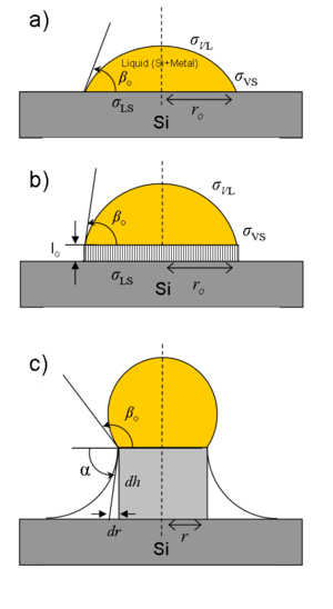
The materials system used, as well as the cleanliness of the vacuum system and therefore the amount of contamination and/or the presence of oxide layers at the droplet and wafer surface during the experiment, both greatly influence the absolute magnitude of the forces present at the droplet/surface interface and, in turn, determine the shape of the droplets. The shape of the droplet, i.e. the contact angle (β0, see Figure 4) can, be modeled mathematically, however, the actual forces present during growth are extremely difficult to measure experimentally. Nevertheless, the shape of a catalyst particle at the surface of a crystalline substrate is determined by a balance of the forces of surface tension and the liquid–solid interface tension. The radius of the droplet varies with the contact angle as:
where r0 is the radius of the contact area and β0 is defined by a modified Young’s equation:
,
It is dependent on the surface (σs) and liquid–solid interface (σls) tensions, as well as an additional line tension (τ) which comes into effect when the initial radius of the droplet is small (nanosized). As a nanowire begins to grow, its height increases by an amount dh and the radius of the contact area decreases by an amount dr (see Figure 4). As the growth continues, the inclination angle at the base of the nanowires (α, set as zero before whisker growth) increases, as does β0:
.
The line tension therefore greatly influences the catalyst contact area. The most import result from this conclusion is that different line tensions will result in different growth modes. If the line tensions are too large, nanohillock growth will result and thus stop the growth.
Nanowhisker diameter
The diameter of the nanowire which is grown depends upon the properties of the alloy droplet. The growth of nano-sized wires requires nano-size droplets to be prepared on the substrate. In an equilibrium situation this is not possible as the minimum radius of a metal droplet is given by[4]
where Vl is the molar volume of the droplet, σlv the liquid-vapor surface energy, and s is the degree of supersaturation[5] of the vapor. This equations restricts the minimum diameter of the droplet, and of any crystals which can be grown from it, under typically conditions to well above the nanometer level. Several techniques to generate smaller droplets have been developed, including the use of monodispersed nanoparticles spread in low dilution on the substrate, and the laser ablation of a substrate-catalyst mixture so to form a plasma which allows well-separated nanoclusters of the catalyst to form as the systems cools.[6]
Whisker growth kinetics
During VLS whisker growth, the rate at which whiskers grow is dependent on the whisker diameter: the larger the whisker diameter, the faster the nanowire grows axially. This is because the supersaturation of the metal-alloy catalyst () is the main driving force for nanowhisker growth and decreases with decreasing whisker diameter (also known as the Gibbs-Thomson effect):
.
Again, Δµ is the main driving force for nanowhisker growth (the supersaturation of the metal droplet). More specifically, Δµ0 is the difference between the chemical potential of the depositing species (Si in the above example) in the vapor and solid whisker phase. Δµ0 is the initial difference proceeding whisker growth (when ), while is the atomic volume of Si and the specific free energy of the wire surface. Examination of the above equation, indeed reveals that small diameters (100 nm) exhibit small driving forces for whisker growth while large wire diameters exhibit large driving forces.
Related growth techniques
Laser-assisted growth
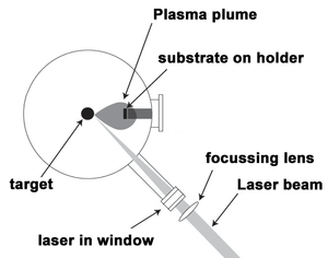
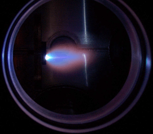
Involves the removal of material from metal-containing solid targets by irradiating the surface with high-powered (~100 mJ/pulse) short (10 Hz) laser pulses, usually with wavelengths in the ultraviolet (UV) region of the light spectrum. When such a laser pulse is adsorbed by a solid target, material from the surface region of the target absorbs the laser energy and either (a) evaporates or sublimates from the surface or is (b) converted into a plasma (see laser ablation). These particles are easily transferred to the substrate where they can nucleate and grow into nanowires. The laser-assisted growth technique is particularly useful for growing nanowires with high melting temperatures, multicomponent or doped nanowires, as well as nanowires with extremely high crystalline quality. The high intensity of the laser pulse incident at the target allows the deposition of high melting point materials, without having to try to evaporate the material using extremely high temperature resistive or electron bombardment heating. Furthermore, targets can simply be made from a mixture of materials or even a liquid. Finally, the plasma formed during the laser absorption process allows for the deposition of charged particles as well as a catalytic means to lower the activation barrier of reactions between target constituents.
Thermal evaporation
Some very interesting nanowires microstructures can be obtained by simply thermally evaporating solid materials. This technique can be carried out in a relatively simple setup composed of a dual-zone vacuum furnace. The hot end of the furnace contains the evaporating source material, while the evaporated particles are carrier downstream, (by way of a carrier gas) to the colder end of the furnace where they can absorb, nucleate, and grow on a desired substrate.
Metal-catalyzed molecular beam epitaxy
Molecular beam epitaxy (MBE) has been used since 2000 to create high-quality semiconductor wires based on the VLS growth mechanism. However, in metal-catalyzed MBE the metal particles do not catalyze a reaction between precursors but rather adsorb vapor phase particles. This is because the chemical potential of the vapor can be drastically lowered by entering the liquid phase.
MBE is carried out under ultra-high vacuum (UHV) conditions where the mean-free-path (distance between collisions) of source atoms or molecules is on the order of meters. Therefore, evaporated source atoms (from, say, an effusion cell) act as a beam of particles directed towards the substrate. The growth rate of the process is very slow, the deposition conditions are very clean, and as a result four superior capabilities arise, when compared to other deposition methods:
- UHV conditions minimize the amount of oxidation/contamination of the growing structures
- Relatively low growth temperatures prevent interdiffusion (mixing) of nano-sized heterostructures
- Very thin-film analysis techniques can be used in-situ (during growth), such as reflection high energy electron diffraction (RHEED) to monitor the microstructure at the surface of the substrate as well as the chemical composition, using Auger electron spectroscopy.
References
- Wagner, R. S.; Ellis, W. C. (1964). "Vapor-liquid-solid mechanism of single crystal growth". Appl. Phys. Lett. 4 (5): 89. doi:10.1063/1.1753975.
- Lu, Yicheng; Zhong, Jian (2004). Todd Steiner (ed.). Semiconductor Nanostructures for Optoelectronic Applications. Norwood, MA: Artech House, Inc. pp. 191–192. ISBN 978-1-58053-751-3.
- Wagner, R. S.; Albert P. Levitt (1975). Whisker Technology. Wiley – Interscience – New York. ISBN 0-471-53150-2.
- Huang, M. H.; Wu, Y; Feick, H; Tran, N.; Weber, E.; Yang, P. (2001). "Catalytic Growth of Zinc Oxide Nanowires by Vapor Transport". Adv. Mater. 13 (2): 113–116. doi:10.1002/1521-4095(200101)13:2<113::aid-adma113>3.0.co;2-h.
- Wang, Ji-Tao (2002). Nonequilibrium Nondissipative Thermodynamics: With Application to Low-pressure Diamond Synthesis. Berlin: Springer Verlag. p. 65. ISBN 978-3-540-42802-2.
- Bhushan, Bharat. Springer Handbook of Nanotechnology. Berlin: Springer-Verlag. p. 105. ISBN 3-540-01218-4.