Stripboard
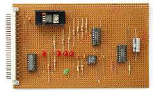
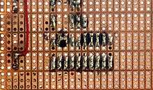
Stripboard is the generic name for a widely used type of electronics prototyping board characterized by a 0.1 inches (2.54 mm) regular (rectangular) grid of holes, with wide parallel strips of copper cladding running in one direction all the way across one side of the board. It is commonly also known by the name of the original product Veroboard, which is a trademark, in the UK, of British company Vero Technologies Ltd and Canadian company Pixel Print Ltd. In using the board, breaks are made in the tracks, usually around holes, to divide the strips into multiple electrical nodes. With care, it is possible to break between holes to allow for components that have two pin rows only one position apart such as twin row headers for IDCs.

Stripboard is not designed for surface-mount components, though it is possible to mount many such components on the track side, particularly if tracks are cut/shaped with a knife or small cutting disc in a rotary tool.
Variations
Stripboard is available from many vendors. All versions have copper strips on one side. Some are made using printed circuit board etching and drilling techniques, although some have milled strips and punched holes. The original Veroboard used FR-2 synthetic-resin-bonded paper (SRBP) (also known as phenolic board) as the base board material. Some versions of stripboard now use higher quality FR-4 (fiberglass-reinforced epoxy laminate) material.[1]
Hole spacing
Stripboard holes are drilled on 0.1 inches (2.54 mm) centers. This spacing allows components having pins with a 0.1 inches (2.54 mm) spacing to be inserted. Compatible parts include DIP ICs, sockets for ICs, some types of connectors, and other devices.
Stripboards have evolved over time into several variants and related products. For example, a larger version using a 0.15 inch (3.81 mm) grid and larger holes is available, but is generally less popular (presumably because it does not match up with standard IC pin spacing).
Board dimensions
Stripboard is available in a variety of sizes. One common size (at least in the United Kingdom) is 160 mm x 100 mm.[2]
Assemblies

The components are usually placed on the plain side of the board, with their leads protruding through the holes. The leads are then soldered to the copper tracks on the other side of the board to make the desired connections, and any excess wire is cut off. The continuous tracks may be easily and neatly cut as desired to form breaks between conductors using a 3 mm twist drill, a hand cutter made for the purpose, or a knife. Tracks may be linked up on either side of the board using wire. With practice, very neat and reliable assemblies can be created, though such a method is labour-intensive and therefore unsuitable for production assemblies except in very small quantity.
External wire connections to the board are made either by soldering the wires through the holes or, for wires too thick to pass through the holes, by soldering them to specially made pins called Veropins which fit tightly into the holes. Alternatively, some types of connectors have a suitable pin spacing to be inserted directly into the board.
Comparison with other systems
Wire wrap
For high density prototyping, especially of digital circuits, wire wrap is faster and more reliable than Stripboard for experienced personnel.[3]
Breadboard
Veroboard is similar in concept and usage to a plug-in breadboard, but is cheaper and more permanent—connections are soldered and while some limited reuse may be possible, more than a few cycles of soldering and desoldering are likely to render both the components and the board unusable. In contrast, breadboard connections are held by friction, and the breadboard can be reused many times. However, a breadboard is not very suitable for prototyping that needs to remain in a set configuration for an appreciable period of time nor for physical mock-ups containing a working circuit or for any environment subject to vibration or movement.
Prototype boards
Stripboards have further evolved into a larger class of prototype boards, available in different shapes and sizes, with different conductive trace layouts.
TriPad

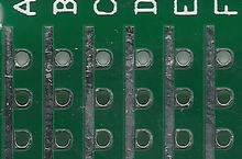
For example, one variant is called a TriPad board. This is similar to stripboard, except that the conductive tracks do not run continuously along the board but are broken into sections, each of which spans three holes. This allows the legs of two or three components to be easily linked together in the circuit conveniently without the need for track breaks to be made. However, in order to link more than three holes together, wire links or bridges must be formed and this can result in a less compact layout than is possible with ordinary stripboard.
Perf+

Another variant is Perf+.[4] This is best described as a selective stripboard. Instead of having all the holes connected together in a strip, a Perf+ board can have holes connected to the bus using a small dab of solder. On the other side the busses run in another direction, allowing compact layouts of complicated circuits by passing signals over each other on different layers of the board.
Other

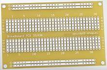
Other prototype board variants have generic layouts to simplify building prototypes with integrated circuits, typically in DIP shapes, or with transistors (pads forming triangles). In particular, some boards mimic the layout of breadboards, to simplify moving a non-permanent prototype on a breadboard to a permanent construction on a PCB. Some types of boards have patterns for connectors on the periphery, like DB9 or IDC headers, to allow connectors with non-standard pin spacings to be easily used.[5] Some come in special physical shapes, to be used to prototype plug-in boards for computer bus systems.
See also
References
| Wikimedia Commons has media related to Stripboard. |
- BusBoard Prototype Systems Ltd. "ST3U StripBoard Datasheet" Retrieved on 2010-10-20. Archived 2011-09-11 at the Wayback Machine
- Prototype and development boards from RS Components The board size with the largest number of products listed is 160 mm x 100 mm.
- Bilotta, Anthony J.: Connections in Electronic Assemblies. Marcel Dekker: 1985. ISBN 0-8247-7319-5
- Original Kickstarter for Perf+. "Perf+ the perfboard reinvented" Retrieved on 2015-4-17.
- BusBoard Prototype Systems Ltd. "PR3UC ProtoBoard With Connectors Datasheet" Retrieved on 2010-10-20.