Resonant-tunneling diode
A resonant-tunneling diode (RTD) is a diode with a resonant-tunneling structure in which electrons can tunnel through some resonant states at certain energy levels. The current–voltage characteristic often exhibits negative differential resistance regions.
All types of tunneling diodes make use of quantum mechanical tunneling. Characteristic to the current–voltage relationship of a tunneling diode is the presence of one or more negative differential resistance regions, which enables many unique applications. Tunneling diodes can be very compact and are also capable of ultra-high-speed operation because the quantum tunneling effect through the very thin layers is a very fast process. One area of active research is directed toward building oscillators and switching devices that can operate at terahertz frequencies.[1]
Introduction

An RTD can be fabricated using many different types of materials (such as III–V, type IV, II–VI semiconductor) and different types of resonant tunneling structures, such as the heavily doped p–n junction in Esaki diodes, double barrier, triple barrier, quantum well, or quantum wire. The structure and fabrication process of Si/SiGe resonant interband tunneling diodes are suitable for integration with modern Si complementary metal–oxide–semiconductor (CMOS) and Si/SiGe heterojunction bipolar technology.
One type of RTDs is formed as a single quantum well structure surrounded by very thin layer barriers. This structure is called a double barrier structure. Carriers such as electrons and holes can only have discrete energy values inside the quantum well. When a voltage is placed across an RTD, a terahertz wave is emitted, which is why the energy value inside the quantum well is equal to that of the emitter side. As voltage is increased, the terahertz wave dies out because the energy value in the quantum well is outside the emitter side energy.
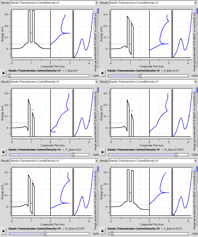
Another feature seen in RTD structures is the negative resistance on application of bias as can be seen in the image generated from Nanohub. The forming of negative resistance will be examined in detail in operation section below.
This structure can be grown by molecular beam heteroepitaxy. GaAs and AlAs in particular are used to form this structure. AlAs/InGaAs or InAlAs/InGaAs can be used.
The operation of electronic circuits containing RTDs can be described by a Liénard system of equations, which are a generalization of the Van der Pol oscillator equation.[2][3][4]
Operation
The following process is also illustrated from rightside figure. Depending on the number of barriers and number of confined states inside the well, the process described below could be repeated.
Positive resistance region
For low bias, as the bias increase, 1st confined state between the potential barriers is getting closer to the source Fermi level, so the current it carries increases.
Negative resistance region
As bias increases further, the 1st confined state becomes lower in energy and gradually goes into the energy range of bandgap, so the current it carries decreases. At this time, the 2nd confined state is still too high above in energy to conduct significant current.
2nd positive resistance region
Similar to the first region, as the 2nd confined state becomes closer and closer to source Fermi level, it carries more current, causing the total current to increase again.
Intraband resonant tunneling

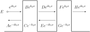
In quantum tunneling through a single barrier, the transmission coefficient, or the tunneling probability, is always less than one (for incoming particle energy less than the potential barrier height). Considering a potential profile which contains two barriers (which are located close to each other), one can calculate the transmission coefficient (as a function of the incoming particle energy) using any of the standard methods.
Tunneling through a double barrier was first solved in the Wentzel-Kramers-Brillouin (WKB) approximation by David Bohm in 1951, who pointed out the resonances in the transmission coefficient occur at certain incident electron energies. It turns out that, for certain energies, the transmission coefficient is equal to one, i.e. the double barrier is totally transparent for particle transmission. This phenomenon is called resonant tunneling.[5] It is interesting that while the transmission coefficient of a potential barrier is always lower than one (and decreases with increasing barrier height and width), two barriers in a row can be completely transparent for certain energies of the incident particle.
Later, in 1964, L. V. Iogansen discussed the possibility of resonant transmission of an electron through double barriers formed in semiconductor crystals.[6] In the early 1970s, Tsu, Esaki, and Chang computed the two terminal current-voltage (I-V) characteristic of a finite superlattice, and predicted that resonances could be observed not only in the transmission coefficient but also in the I-V characteristic.[7] Resonant tunneling also occurs in potential profiles with more than two barriers. Advances in the MBE technique led to observation of negative differential conductance (NDC) at terahertz frequencies, as reported by Sollner et al. in the early 1980s.[8] This triggered a considerable research effort to study tunneling through multi-barrier structures.
The potential profiles required for resonant tunneling can be realized in semiconductor system using heterojunctions which utilize semiconductors of different types to create potential barriers or wells in the conduction band or the valence band.
III-V resonant tunneling diodes
Resonant tunneling diodes are typically realized in III-V compound material systems, where heterojunctions made up of various III-V compound semiconductors are used to create the double or multiple potential barriers in the conduction band or valence band. Reasonably high performance III-V resonant tunneling diodes have been realized. Such devices have not entered mainstream applications yet because the processing of III-V materials is incompatible with Si CMOS technology and the cost is high.
Most of semiconductor optoelectronics use III-V semiconductors and so it is possible to combine III-V RTDs to make OptoElectronic Integrated Circuits (OEICS) that use the negative differential resistance of the RTD to provide electrical gain for optoelectronic devices.[9][10] Recently, the device to device variability in an RTDs current-voltage characteristic has been used as a way to uniquely identify electronic devices, in what is known as a quantum confinement physical unclonable function (QC-PUF).[11]
Si/SiGe resonant tunneling diodes
Resonant tunneling diodes can also be realized using the Si/SiGe materials system. Both hole tunneling and electron tunneling have been observed. However, the performance of Si/SiGe resonant tunneling diodes was limited due to the limited conduction band and valence band discontinuities between Si and SiGe alloys. Resonant tunneling of holes through Si/SiGe heterojunctions was attempted first because of the typically relatively larger valence band discontinuity in Si/SiGe heterojunctions than the conduction band discontinuity for (compressively) strained Si1−xGex layers grown on Si substrates. Negative differential resistance was only observed at low temperatures but not at room temperature.[12] Resonant tunneling of electrons through Si/SiGe heterojunctions was obtained later, with a limited peak-to-valley current ratio (PVCR) of 1.2 at room temperature.[13] Subsequent developments have realized Si/SiGe RTDs (electron tunneling) with a PVCR of 2.9 with a PCD of 4.3 kA/cm2 [14] and a PVCR of 2.43 with a PCD of 282 kA/cm2 at room temperature.[15]
Interband resonant tunneling diodes
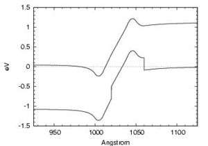
Resonant interband tunneling diodes (RITDs) combine the structures and behaviors of both intraband resonant tunneling diodes (RTDs) and conventional interband tunneling diodes, in which electronic transitions occur between the energy levels in the quantum wells in the conduction band and that in the valence band.[16][17] Like resonant tunneling diodes, resonant interband tunneling diodes can be realized in both the III-V and Si/SiGe materials systems.
III-V RITDs
In the III-V materials system, InAlAs/InGaAs RITDs with peak-to-valley current ratios (PVCRs) higher than 70 and as high as 144 at room temperature and Sb-based RITDs with room temperature PVCR as high as 20 have been obtained.[18][19][20] The main drawback of III-V RITDs is the use of III-V materials whose processing is incompatible with Si processing and is expensive.
Si/SiGe RITDs


In Si/SiGe materials system, Si/SiGe resonant interband tunneling diodes have also been developed which have the potential of being integrated into the mainstream Si integrated circuits technology.[21]
Structure
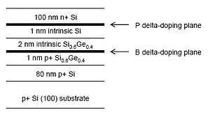
The five key points to the design are: (i) an intrinsic tunneling barrier, (ii) delta-doped injectors, (iii) offset of the delta-doping planes from the heterojunction interfaces, (iv) low temperature molecular beam epitaxial growth (LTMBE), and (v) postgrowth rapid thermal annealing (RTA) for activation of dopants and reduction of density of point defects.[21]
Performance
A minimum PVCR of about 3 is needed for typical circuit applications. Low current density Si/SiGe RITDs are suitable for low-power memory applications, and high current density tunnel diodes are needed for high-speed digital/mixed-signal applications. Si/SiGe RITDs have been engineered to have room temperature PVCRs up to 4.0.[22] The same structure was duplicated by another research group using a different MBE system, and PVCRs of up to 6.0 have been obtained.[23] In terms of peak current density, peak current densities ranging from as low as 20 mA/cm2 and as high as 218 kA/cm2, spanning seven orders of magnitude, have been achieved.[24] A resistive cut-off frequency of 20.2 GHz has been realized on photolithography defined SiGe RITD followed by wet etching for further reducing the diode size, which should be able to improve when even smaller RITDs are fabricated using techniques such as electron beam lithography.[25]
Applications
In addition to the realization of integration with Si CMOS and SiGe heterojunction bipolar transistors that is discussed in the next section, other applications of SiGe RITD have been demonstrated using breadboard circuits, including multi-state logic.[26]
Integration with Si/SiGe CMOS and heterojunction bipolar transistors
Integration of Si/SiGe RITDs with Si CMOS has been demonstrated.[27] Vertical integration of Si/SiGe RITD and SiGe heterojunction bipolar transistors was also demonstrated, realizing a 3-terminal negative differential resistance circuit element with adjustable peak-to-valley current ratio.[28] These results indicate that Si/SiGe RITDs is a promising candidate of being integrated with the Si integrated circuit technology.
References
- Saeedkia, D. (2013). Handbook of Terahertz Technology for Imaging, Sensing and Communications. Elsevier. p. 429. ISBN 978-0857096494.
- Slight, Thomas J.; Romeira, Bruno; Wang, Liquan; Figueiredo, JosÉ M. L.; Wasige, Edward; Ironside, Charles N. (2008). "A Liénard Oscillator Resonant Tunnelling Diode-Laser Diode Hybrid Integrated Circuit: Model and Experiment" (PDF). IEEE Journal of Quantum Electronics. 44 (12): 1158. Bibcode:2008IJQE...44.1158S. doi:10.1109/JQE.2008.2000924.
- Romeira, B.; Slight, J.M.L.; Figueiredo, T.J.; Wasige, L.; Wang, E.; Quintana, C.N.; Ironside, J.M.; Avedillo, M.J. (2008). "Synchronisation and chaos in a laser diode driven by a resonant tunnelling diode". IET Optoelectronics. 2 (6): 211. doi:10.1049/iet-opt:20080024.
- Romeira, B.; Figueiredo, J. M. L.; Slight, T. J.; Wang, L.; Wasige, E.; Ironside, C. N.; Quintana, J. M.; Avedillo, M. J. (May 4–9, 2008). "Observation of Frequency Division and Chaos Behavior in a Laser Diode driven by a Resonant Tunneling Diode". Conference on Lasers and Electro-Optics and Quantum Electronics and Laser Science (CLEO/QELS 2008), San Jose, California: 1–2. doi:10.1109/CLEO.2008.4551318. ISBN 978-1-55752-859-9.
- David Bohm, Quantum Theory, Prentice-Hall, New York, 1951.
- L. V. Iogansen, "The possibility of resonance transmission of electrons in crystals through a system of barriers," Soviet Physics JETP, 1964, 18, pp. 146.
- Tsu, R.; Esaki, L. (1973). "Tunneling in a finite superlattice". Applied Physics Letters. 22 (11): 562. Bibcode:1973ApPhL..22..562T. doi:10.1063/1.1654509.
- Sollner, T. C. L. G.; Goodhue, W. D.; Tannenwald, P. E.; Parker, C. D.; Peck, D. D. (1983). "Resonant tunneling through quantum wells at frequencies up to 2.5 THz". Applied Physics Letters. 43 (6): 588. Bibcode:1983ApPhL..43..588S. doi:10.1063/1.94434.
- Slight, T.J.; Ironside, C.N. (2007). "Investigation Into the Integration of a Resonant Tunnelling Diode and an Optical Communications Laser: Model and Experiment" (PDF). IEEE Journal of Quantum Electronics. 43 (7): 580. Bibcode:2007IJQE...43..580S. doi:10.1109/JQE.2007.898847.
- Figueiredo, J.M.L.; Romeira, B.; Slight, T.J.; Wang, L.; Wasige, E.; Ironside, C.N. (2008). "Self-oscillation and period adding from resonant tunnelling diode–laser diode circuit" (PDF). Electronics Letters. 44 (14): 876. doi:10.1049/el:20080350.
- Roberts, J.; Bagci, I. E.; Zawawi, M. A. M.; Sexton, J.; Hulbert, N.; Noori, Y. J.; Young, M. P.; Woodhead, C. S.; Missous, M.; Migliorato, M. A.; Roedig, U.; Young, R. J. (2015-11-10). "Using Quantum Confinement to Uniquely Identify Devices". Scientific Reports. 5: 16456. arXiv:1502.06523. Bibcode:2015NatSR...516456R. doi:10.1038/srep16456. PMC 4639737. PMID 26553435.
- Gennser, Ulf; Kesan, V. P.; Iyer, S. S.; Bucelot, T. J.; Yang, E. S. (1990). "Resonant tunneling of holes through silicon barriers". Journal of Vacuum Science and Technology B. 8 (2): 210. Bibcode:1990JVSTB...8..210G. doi:10.1116/1.584811.
- Ismail, K.; Meyerson, B. S.; Wang, P. J. (1991). "Electron resonant tunneling in Si/SiGe double barrier diodes". Applied Physics Letters. 59 (8): 973. Bibcode:1991ApPhL..59..973I. doi:10.1063/1.106319.
- P. See; D.J. Paul; B. Hollander; S. Mantl; I. V. Zozoulenko & K.-F. Berggren (2001). "High Performance Si/Si1−xGex Resonant Tunneling Diodes". IEEE Electron Device Letters. 22 (4): 182. Bibcode:2001IEDL...22..182S. doi:10.1109/55.915607.
- P. See & D.J. Paul (2001). "The scaled performance of Si/Si1−xGex resonant tunneling diodes". IEEE Electron Device Letters. 22 (12): 582. Bibcode:2001IEDL...22..582S. doi:10.1109/55.974584.
- Sweeny, Mark; Xu, Jingming (1989). "Resonant interband tunnel diodes". Applied Physics Letters. 54 (6): 546. Bibcode:1989ApPhL..54..546S. doi:10.1063/1.100926.
- Kwok K. Ng (2002). Complete Guide to Semiconductor Devices (2 ed.). Wiley-Interscience.
- Day, D. J.; Chung, Y.; Webb, C.; Eckstein, J. N.; Xu, J. M.; Sweeny, M. (1990). "Double quantum well resonant tunneling diodes". Applied Physics Letters. 57 (12): 1260. Bibcode:1990ApPhL..57.1260D. doi:10.1063/1.103503.
- Tsai, H.H.; Su, Y.K.; Lin, H.H.; Wang, R.L.; Lee, T.L. (1994). "P-N double quantum well resonant interband tunneling diode with peak-to-valley current ratio of 144 at room temperature". IEEE Electron Device Letters. 15 (9): 357. Bibcode:1994IEDL...15..357T. doi:10.1109/55.311133.
- Söderström, J. R.; Chow, D. H.; McGill, T. C. (1989). "New negative differential resistance device based on resonant interband tunneling". Applied Physics Letters. 55 (11): 1094. Bibcode:1989ApPhL..55.1094S. doi:10.1063/1.101715.
- Rommel, Sean L.; Dillon, Thomas E.; Dashiell, M. W.; Feng, H.; Kolodzey, J.; Berger, Paul R.; Thompson, Phillip E.; Hobart, Karl D.; Lake, Roger; Seabaugh, Alan C.; Klimeck, Gerhard; Blanks, Daniel K. (1998). "Room temperature operation of epitaxially grown Si/Si[sub 0.5]Ge[sub 0.5]/Si resonant interband tunneling diodes". Applied Physics Letters. 73 (15): 2191. Bibcode:1998ApPhL..73.2191R. doi:10.1063/1.122419.
- Park, S.-Y.; Chung, S.-Y.; Berger, P.R.; Yu, R.; Thompson, P.E. (2006). "Low sidewall damage plasma etching using ICP-RIE with HBr chemistry of Si∕SiGe resonant interband tunnel diodes". Electronics Letters. 42 (12): 719. doi:10.1049/el:20060323.
- Duschl, R; Eberl, K (2000). "Physics and applications of Si/SiGe/Si resonant interband tunneling diodes". Thin Solid Films. 380 (1–2): 151–153. Bibcode:2000TSF...380..151D. doi:10.1016/S0040-6090(00)01491-7.
- Jin, N.; Chung, S.-Y.; Yu, R.; Heyns, R.M.; Berger, P.R.; Thompson, P.E. (2006). "The Effect of Spacer Thicknesses on Si-Based Resonant Interband Tunneling Diode Performance and Their Application to Low-Power Tunneling Diode SRAM Circuits". IEEE Transactions on Electron Devices. 53 (9): 2243. Bibcode:2006ITED...53.2243J. doi:10.1109/TED.2006.879678.
- S.Y. Chung; R. Yu; N. Jin; S.Y. Park; P.R. Berger & P.E. Thompson (2006). "Si/SiGe Resonant Interband Tunnel Diode with fr0 20.2 GHz and Peak Current Density 218 kA/cm2 for K-band Mixed-Signal Applications". IEEE Electron Device Letters. 27 (5): 364. Bibcode:2006IEDL...27..364C. doi:10.1109/LED.2006.873379.
- N. Jin; S.Y. Chung; R.M. Heyns; and P.R. Berger; R. Yu; P.E. Thompson & S.L. Rommel (2004). "Tri-State Logic Using Vertically Integrated Si Resonant Interband Tunneling Diodes with Double NDR". IEEE Electron Device Letters. 25 (9): 646. Bibcode:2004IEDL...25..646J. doi:10.1109/LED.2004.833845.
- S. Sudirgo, D.J. Pawlik, S.K. Kurinec, P.E. Thompson, J.W. Daulton, S.Y. Park, R. Yu, P.R. Berger, and S.L. Rommel, NMOS/SiGe Resonant Interband Tunneling Diode Static Random Access Memory, 64th Device Research Conference Conference Digest, page 265, June 26–28, 2006, The Pennsylvania State University, University Park, PA.
- Chung, Sung-Yong; Jin, Niu; Berger, Paul R.; Yu, Ronghua; Thompson, Phillip E.; Lake, Roger; Rommel, Sean L.; Kurinec, Santosh K. (2004). "Three-terminal Si-based negative differential resistance circuit element with adjustable peak-to-valley current ratios using a monolithic vertical integration". Applied Physics Letters. 84 (14): 2688. Bibcode:2004ApPhL..84.2688C. doi:10.1063/1.1690109.
External links
- For information on Optoelectronic applications of RTDs see http://userweb.elec.gla.ac.uk/i/ironside/RTD/RTDOpto.html.
- Resonant Tunneling Diode Simulation Tool on Nanohub enables the simulation of resonant tunneling diodes under realistic bias conditions for realistically extended devices.