Nickel silicide
Nickel silicides include several intermetallic compounds of nickel and silicon. Nickel silicides are important in microelectronics as they form at junctions of nickel and silicon. Additionally thin layers of nickel silicides may have application in imparting surface resistance to nickel alloys.
 | |
| Identifiers | |
|---|---|
3D model (JSmol) |
|
| ChemSpider | |
| EC Number |
|
PubChem CID |
|
| |
| |
| Properties | |
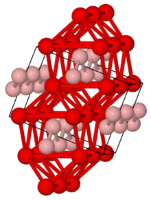
| Ni2Si | |
| Molar mass | 145.473 g/mol[1] |
| Density | 7.40 g/cm3[1] |
| Melting point | 1,255 °C (2,291 °F; 1,528 K)[1] |
| Structure[2] | |
| Orthorhombic, oP12 | |
| Pnma, No. 62 | |
a = 0.502 nm, b = 0.374 nm, c = 0.708 nm | |
Formula units (Z) |
4 |
Except where otherwise noted, data are given for materials in their standard state (at 25 °C [77 °F], 100 kPa). | |
| Infobox references | |
 | |
| Identifiers | |
|---|---|
3D model (JSmol) |
|
PubChem CID |
|
| |
| |
| Properties | |
| NiSi | |
| Molar mass | 86.778 g/mol |
| Structure[3] | |
| Orthorphomic, oP8 | |
| Pnma, No. 62 | |
a = 0.519 nm, b = 0.333 nm, c = 0.5628 nm | |
Formula units (Z) |
4 |
Except where otherwise noted, data are given for materials in their standard state (at 25 °C [77 °F], 100 kPa). | |
| Infobox references | |
 | |
| Identifiers | |
|---|---|
| Properties | |
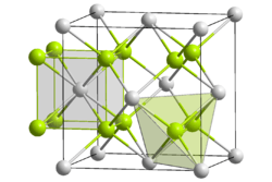
| NiSi2 | |
| Molar mass | 114.864 g/mol[1] |
| Density | 7.83 g/cm3[1] |
| Melting point | 993 °C (1,819 °F; 1,266 K)[1] |
| Structure[4] | |
| Cubic, cF12 | |
| Fm3m, No. 225 | |
a = 0.5406 nm | |
Formula units (Z) |
4 |
Except where otherwise noted, data are given for materials in their standard state (at 25 °C [77 °F], 100 kPa). | |
| Infobox references | |
Compounds
Nickel silicides include Ni3Si, Ni31Si12, Ni2Si, Ni3Si2, NiSi and NiSi2.[5] Ni31Si12, Ni2Si, and NiSi have congruent melting points; the others form via a peritectic transformation. The silicides can be made via fusion or solid state reaction between the elements, diffusion at a junction of the two elements, and other methods including ion beam mixing.
Properties
Nickel silicides are generally chemically and thermally stable. They have low electrical resistivity; with NiSi 10.5–18 μΩ·cm, Ni2Si 24–30 μΩ·cm, NiSi2 34–50 μΩ·cm; nickel-rich silicides have higher resistivity rising to 90–150 μΩ·cm in Ni31Si12.
Uses
Microelectronics
Nickel silicides are important in microelectronic devices – specific silicides are good conductors, with NiSi having a conductivity approaching that of elemental nickel. With silicon carbide as the semiconductor nickel reacts at elevated temperatures to form nickel silicides and carbon.
Other
Nickel silicides have potential as coatings for nickel-based superalloys and stainless steel, due to their corrosion, oxidation, and wear resistance. NiSi has been investigated as a hydrogenation catalyst for unsaturated hydrocarbons.[6]
See also
- J. Marvin Herndon, who promoted a theory that the earth's core is nickel silicide
- Titanium disilicide, also used in microelectronics
- Salicide, self-aligned silicides
References
- Haynes, William M., ed. (2011). CRC Handbook of Chemistry and Physics (92nd ed.). CRC Press. p. 4.77. ISBN 978-1439855119.
- El Boragy M., Rajasekharan T.P., Schubert K. (1982). Z. Metallkd., 73, 193–197
- Wopersnow W., Schubert K. (1976) Z. Metallkd., 67, 807–810
- Beck, U.; Neumann, H.-G.; Becherer, G. (1973). "Phasenbildung in Ni/Si-Schichten". Kristall und Technik. 8 (10): 1125–1129. doi:10.1002/crat.19730081005.
- Dahal, Ashutosh; Gunasekera, Jagath; Harringer, Leland; Singh, Deepak K.; Singh, David J. (July 2016), "Metallic nickel silicides: Experiments and theory for NiSi and first principles calculations for other phases", Journal of Alloys and Compounds, 672: 110–116, arXiv:1602.05840, doi:10.1016/j.jallcom.2016.02.133
- Itahara, Hiroshi; Simanullang, Wiyanti F.; Takahashi, Naoko; Kosaka, Satoru; Furukawa, Shinya (2019), "Na-Melt Synthesis of Fine Ni3Si Powders as a Hydrogenation Catalyst", Inorganic Chemistry, 58 (9): 5406–5409, doi:10.1021/acs.inorgchem.9b00521, PMID 30983337
Further reading
- Lavoie, C.; d’Heurle, F.M.; Detavernier, C.; Cabral, C. (Nov 2003), "Towards implementation of a nickel silicide process for CMOS technologies", Microelectronic Engineering, 70 (2–4): 144–157, doi:10.1016/S0167-9317(03)00380-0