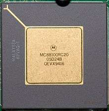
Motorola 88100
The MC88100 is a microprocessor developed by Motorola that implemented 88000 instruction set architecture. Announced in 1988, the MC88100 was the first 88000 implementation. It was succeeded by the MC88110 in the early 1990s.
The microprocessor was a superscalar design with multiple integer and floating-point units that executed instructions in-order. The MC88100 had separate instruction and data caches. These caches were implemented with the MC88200 integrated circuit, which contains a memory management unit and an amount of cache. The MC88100 requires two of these devices for each cache, and additional MC88200s could be added to increase the size of the caches.
This partitioned scheme was chosen to provide system flexibility, the amount of cache could be varied depending on the price point. In practice, these additional chips required more space on the circuit board and the buses between the MC88200s and MC88100 added complexity and cost.
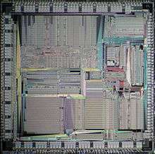
The MC88100 contained 165,000 transistors and the MC88200 750,000 transistors. Both were fabricated by Motorola in its 1.5 μm complementary metal–oxide–semiconductor process.
The MC88100 was ultimately commercially unsuccessful. This was due to a number of reasons, including requirement of MC88200s, but was mostly due to Motorola being a vendor of the highly successful 68000 family. As the 68000 division viewed the 88000 as a competitor, they forced the MC88100 to be priced unacceptably high for a volume part. The part did find use in the high-end embedded market, in Motorola's own computers, and in large computers from companies such as Data General and the Unisys S-8400 Unix Servers.
Design
Programming model and register set
The programming model and register set of the MC88100 is remarkably similar to DLX (And by extension, RISC-V) based CPUs, with 32 General-purpose registers (31 writable) and 51 instructions capable of accessing any of the 32 general purpose registers at any time.
Registers
| MC88100 Registers | |||||||||||||||||||||||||||||||||||||||||||||||||||||||||||||||||||||||||||||||||||||||||||||||||||||||||||||||||||||||||||||||||||||||||||||||||||||||||
| |||||||||||||||||||||||||||||||||||||||||||||||||||||||||||||||||||||||||||||||||||||||||||||||||||||||||||||||||||||||||||||||||||||||||||||||||||||||||
The MC88100 is equipped with a total of 64 user accessible registers, 32 of them being Control registers, and can access up to 6 registers (4 read, 2 write) simultaneously. The actual usage of GPR is not enforced by the processor for every register except R1, which is used as a return address.
References
- Furber, Stephen Bo (1989). VLSI RISC Architecture and Organization. CRC Press. pp. 184–192.
- Tabak, Daniel (1990). RISC Systems. Research Studies Press. pp. 121–143.
- Tabak, Daniel (1995). Advanced Microprocessors (2 ed.). McGraw-Hill. pp. 433–434, 437.
- Motorola, inc, ed. (1990). MC88100 Risc Microprocessor User's Manual. Prentice Hall. ISBN 013567090X.
| Authority control |
|
|---|