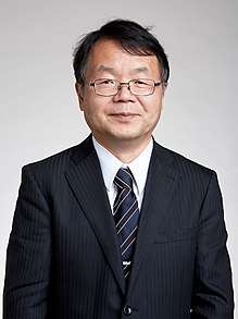
Hideo Hosono
Hideo Hosono (細野秀雄, Hosono Hideo, born September 7, 1953), ForMemRS, is a Japanese material scientist most known for the discovery of iron-based superconductors.[1][2]
Hideo Hosono | |
|---|---|
 Hideo Hosono at the Royal Society admissions day in London, July 2017 | |
| Born | Hideo Hosono September 7, 1953 |
| Nationality | Japan |
| Alma mater | Tokyo Metropolitan University |
| Known for | iron-based superconductors thin-film transistors |
| Awards | Japan Prize Medal of Honor (Purple Ribbon) Research Achievement Award (Japanese Society of Applied Physics) James C. McGroddy Prize for New Materials |
| Scientific career | |
| Fields | Materials science |
| Institutions | Tokyo Institute of Technology Nagoya Institute of Technology |
Career and research
Hosono is also a pioneer in developing transparent oxide semiconductors: he proposed a material design concept for an transparent amorphous oxide semiconductor (TAOS) with large electron mobility, demonstrated the excellent performance of TAOS thin film transistors for next generation displays and successfully converted a cement constituent 12CaO·7Al2O3 into transparent semiconductor, metal, and eventually superconductors.[3][4] [5]
Awards and honors
- 2009 – Bernd T. Matthias Prize for Superconductivity[6]
- 2009 – Medal of Honor (Purple Ribbon)
- 2012 – Nishina Memorial Prize
- 2013 – Thomson Reuters Citation Laureates
- 2015 – Imperial Prize of the Japan Academy
- 2016 – Japan Prize
- 2017 – Elected a Foreign Member of the Royal Society[7]
Selected publications
According to the Web of Science, Hideo Hosono has co-authored 5 articles with more than 1000 citations each (as of September 2019):
- Kamihara, Y.; Watanabe, T.; Hirano, M.; Hosono, H. (2008). "Iron-Based Layered Superconductor La[O1−xFx]FeAs (x = 0.05–0.12) with Tc= 26 K". Journal of the American Chemical Society. 130 (11): 3296–7. doi:10.1021/ja800073m. PMID 18293989.
- Nomura, K.; Ohta, H.; Takagi, A.; Kamiya, T.; Hirano, M.; Hosono, H. (2004). "Room-temperature fabrication of transparent flexible thin-film transistors using amorphous oxide semiconductors". Nature. 432 (7016): 488–92. Bibcode:2004Natur.432..488N. doi:10.1038/nature03090. PMID 15565150.
- Kawazoe, H.; Yasukawa, M.; Hyodo, H.; Kurita, M.; Yanagi, H.; Hosono, H. (1997). "P-type electrical conduction in transparent thin films of CuAlO2". Nature. 389 (6654): 939. Bibcode:1997Natur.389..939K. doi:10.1038/40087.
- Nomura, K; Ohta, H; Ueda, K; Kamiya, T; Hirano, M; Hosono, H (2003). "Thin-film transistor fabricated in single-crystalline transparent oxide semiconductor". Science. 300 (5623): 1269–72. Bibcode:2003Sci...300.1269N. doi:10.1126/science.1083212. JSTOR 3834084. PMID 12764192.
- Kamiya, Toshio; Nomura, Kenji; Hosono, Hideo (2016). "Present status of amorphous In–Ga–Zn–O thin-film transistors". Science and Technology of Advanced Materials. 11 (4): 044305. Bibcode:2010STAdM..11d4305K. doi:10.1088/1468-6996/11/4/044305. PMC 5090337. PMID 27877346.
gollark: Or fastboot.
gollark: I can get *recovery mode*, but only a somewhat broken recovery mode which lets me run shell commands somehow but which does not seem to want to actually boot into system mode, *somehow*.
gollark: I did some things a while ago, forgot about them, rebooted now, and [REDACTED].
gollark: 🐝 the entire android boot process at the same time. It appears that my phone is somewhat apioformed.
gollark: * my `wall`
References
- "Hideo Hosono ScienceWatch.com December 2008". Archived from the original on 2013-10-04.
- Kamihara, Y.; Watanabe, T.; Hirano, M.; Hosono, H. (2008). "Iron-Based Layered Superconductor La[O1−xFx]FeAs (x = 0.05–0.12) with Tc= 26 K". Journal of the American Chemical Society. 130 (11): 3296–7. doi:10.1021/ja800073m. PMID 18293989.
- Hideo Hosono. fpdchina.org
- LaboratoryProfile – Hosono. materia.titech.ac.jp
- Hideo Hosono (2014) "Impression-Inspired Materials Research", Vimeo Youtube.
- Bernd T. Matthias Prize Archived 2017-12-09 at the Wayback Machine. m2s–2015.ch
- "Hideo Hosono ForMemRS". Archived from the original on 2017-05-23.
This article is issued from Wikipedia. The text is licensed under Creative Commons - Attribution - Sharealike. Additional terms may apply for the media files.