Glass frit bonding
Glass frit bonding, also referred to as glass soldering or seal glass bonding, describes a wafer bonding technique with an intermediate glass layer. It is a widely used encapsulation technology for surface micro-machined structures, e.g., accelerometers or gyroscopes.[1] This technique utilizes low melting glass ("glass solder") and therefore provides various advantages including that viscosity of glass decreases with an increase of temperature. The viscous flow of glass has effects to compensate and planarize surface irregularities, convenient for bonding wafers with a high roughness due to plasma etching or deposition. A low viscosity promotes hermetically sealed encapsulation of structures based on a better adaption of the structured shapes.[2] Further, the coefficient of thermal expansion (CTE) of the glass material is adapted to silicon. This results in low stress in the bonded wafer pair.
Glass frit bonding can be used for many surface materials, e.g., silicon with hydrophobic and hydrophilic surface, silicon dioxide, silicon nitride, aluminium, titanium or glass, as long as the CTE are in the same range. This bonding procedure also allows the realization of metallic feedthroughs to contact active structures in the hermetically sealed cavity. Glass frit as a dielectric material does not need additional passivation for preventing leakage currents at process temperatures up to 125 °C.[3]
Following advantages resulting in using glass frit bonding procedure:[4]
- screen printing process applicable on thin, structured wafer
- no electrical potentials during bonding process necessary
- low tension due to low bonding temperature
- selective bonding based on structured intermediate glass layer
- bonding of rough wafer surfaces
- no outgassing after bonding, better chemical durability, higher strength compared to organic adhesives
- high reliability and stable hermetical sealing
- easier process compared to metallic or eutectic layer procedures
Overview
The glass frit bond procedure is used for the encapsulation and mounting of components. The coating of glass frit layers is applied by spin coating for thickness of 5 to 30 μm or commonly by screen printing for thickness of 10 to 30 μm.[5]
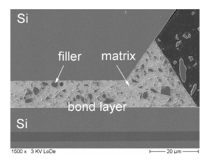
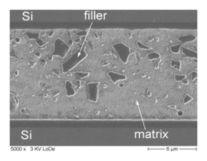
To achieve process temperatures beneath 450 °C leaded glass or lead silicate glass is used. The glass frit is a paste consisting glass powder, organic binder, inorganic fillers and solvents. This low melting glass paste is milled into powder (grain size < 15 μm) and mixed with organic binder forming a printable viscous paste.[3] Inorganic fillers, i.e. cordierite particles (e.g. Mg2Al3 [AlSi5O18]) or barium silicate, are added to the melted glass paste to influence properties, i.e. lowering the mismatch of thermal expansion coefficients between silicon and glass frit.[6] The solvents are used to adjust the viscosity of the organic binder. Several glass frit pastes are commercially available, e.g. FERRO FX-11-0366, and every single one need individual handling after deposition.[4] The choice of the paste depends on various factors, i.e. deposition method, substrate material and process temperatures.[2]
The glass used for MEMS applications consists of particles and lead oxide. Latter lowers the glass transition temperature below 400 °C.[7] The reduction of lead oxide by the silicon leads to the formation of lead precipitations at the silicon-glass interface. Those precipitations decrease the strength of the bond and are reliability risks that have to be considered for the lifetime predictions of the devices.[6]
The printed glass frit structures are heated to form compact glass. The heating process is necessary to drive out the solvents and binder. This results in a subsequent particle fusion of the glass powder. Using mechanical pressure the wafers are bonded at elevated temperatures.[2]
The procedural steps of glass frit bonding are divided into the following:[5]
- Deposition of glass paste
- Burn out and firing (in order to form glass layer)
- Bonding process
- Cooling down
Procedural steps
Glass frit deposition
Screen printing, as a commonly used deposition method, provides a technique of structuring for the glass frit material. This method has the advantage of material deposition on structured cap wafers without any additional processes, i.e. photolithography.[3]
Screen printing enables the possibility of selective bonding. So only in areas where bonding is required the glass frit is deposited.[3]
The risk of glass frit flowing into the structures can be prevented by optimization of the screen printing process. Under high positioning precision the sizes of the structures in the range of 190 μm with a minimum spacing of < 100 μm are achievable. The exact positioning of the screen print structures to the cap wafer are required to ensure an accurate bond. The bonded structures are, dependent on the wettability of the printed surface, 10 to 20% wider than the designed screen.[4]
To ensure a uniform glass thickness, all structures should have the same width. The printed glass frit high is about 30 μm and provides a gap of 5 to 10 μm between the bonded wafers after bonding (compare to cross sectional SEM images).[3] A bond surface activation is not necessary to promote a higher bonding strength.[8]


Thermal conditioning
Thermal conditioning transforms the glass paste into glass layer and is important to prevent voids inside the glass frit layer.[3] The conditioning process consists of:
- Glazing of organic binder and solvents
- Melting of glass particle to compact glass
- Formation of solid connection between glass and wafer surface
The initial step comprises drying for 5 to 7 minutes at 100 to 120 °C in order to diffuse solvents out of the interface. This starts the polymerization of the organic binder. The binder molecules are linked to long-chain polymers what solidifies the paste.[4]
The organic binder of the glass paste has to be burned with heating up to a specific temperature (325 to 350 °C) where the glass is not fully melted for 10 to 20 minutes. This so-called glazing ensures the outgassing of the organic additives.
Further, a pre-melting or sealing step heats the material to the process temperature between 410 and 459 °C for 5 to 10 min. The material fully melts and forms a compact glass without any inclusions. The inorganic fillers are melted down and the properties of the bond glass are fixed.[3] The melting of the glass starts at the silicon-glass interface directed to the glass surface. During the melting process the porosity of the glass eliminates and based on the compression of the intermediate layer the thickness of the glass decreases significantly.[4]
Bonding process
The glass frit bonding, starting with alignment of the wafers, is a thermo-compressive process that takes place in the bonding chamber at specific pressure. Under bonding pressure wafers are heated up to the process temperature around 430 °C for a few minutes.[3] On the one hand a short bonding time causes the glass frit to spread insufficiently, on the other hand a longer bonding time causes the glass frit to be overflown subsequently leaving voids.[8]
The alignment has to be very precise and stable to prevent shifting. This can be realized using clamps or special pressure plates.[3] Shifting can occur through temporarily staggered pressure, not precise vertical pressure based on misalignment of the bonding tools or the difference of thermal expansion between the bonding tools.[4]
During bonding a supporting tool pressure is applied to improve the thermal input into the bonding glass and equal wafer geometry inadmissibility (i.e. bow and warp) supporting wettability.[9] Based on the sufficiently high viscosity of the glass, bonding can take place nearly without pressure.[4]
The bonding temperature needs to be high enough to reduce the viscosity of the glass material and ensures a good wetting of the bond surface, but also low enough to prevent overspreading of the glass frit material. The heating up over 410 °C enables the wetting of the bond surface. A good wetting is indicated by a low edge angle. The atomic wafer surface layers are fused into the glass at an atomic level.[9] This forms a thin glass mixture at the interface which forms the strong bond between the glass and the wafer.[3]
Cooling down
During cooling down under pressure a mechanically strong and hermetically sealed wafer bond is formed.[3] The cooling process leads especially at higher temperatures to thermal stress in the glass frit layer that has to be considered in the lifetime analysis of the bond frame.[7] The wafer pair is removed from the bond chamber at lower temperatures to prevent thermal cracking of the wafers or the bond interface by thermal shocks.[9]
The bonding strength is mainly dependent on the density, the spreading area of the glass frit layer and the surface layer of the bonding interface. It is high enough, around 20 MPa, for most applications and comparable to those achieved with anodic bonding. The hermeticity ensures the correct function and a sufficient reliability of the bond and therefore the product. Further, the bonding yield of glass frit bonded wafers is very high, normally > 90 %.[8]
Examples
Glass frit bonding is used to encapsulate surface micro-machined sensors, i.e. gyroscopes and accelerometers. Other applications are the sealing of absolute pressure sensor cavities, the mounting of optical windows and the capping of thermally active devices.[3]
Technical specifications
| Materials |
Substrate:
Intermediate layer:
|
| Temperature |
|
| Advantages |
|
| Drawbacks |
|
References
- Dresbach, C. and Krombholz, A. and Ebert, M. and Bagdahn, J. (2006). "Mechanical properties of glass frit bonded micro packages". Microsystem Technologies. 12 (5). pp. 473–480. doi:10.1007/s00542-005-0031-9.CS1 maint: multiple names: authors list (link)
- Knechtel, R. (2003). "Glass-Frit-Waferbonden: Verbindungsbildung, technologischer Ablauf und Anwendung". In Gessner, T. (ed.). 6. Chemnitzer Fachtagung Mikromechanik & Mikroelektronik. pp. 79–83.
- Knechtel, R. (2005). "Glass frit bonding: an universal technology for wafer level encapsulation and packaging". Microsystem Technologies. 12. pp. 63–68. doi:10.1007/s00542-005-0022-x.
- Knechtel, R. (2005). Halbleiterwaferbondverbindungen mittels strukturierter Glaszwischenschichten zur Verkapselung oberflächenmikromechanischer Sensoren auf Waferebene (Thesis). ISBN 3-89963-166-8.
- Wiemer, M. and Frömel, J. and Gessner, T. (2003). "Trends der Technologieentwicklung im Bereich Waferbonden". In W. Dötzel (ed.). 6. Chemnitzer Fachtagung Mikromechanik & Mikroelektronik. 6. Technische Universität Chemnitz. pp. 178–188.CS1 maint: multiple names: authors list (link)
- Nötzold, K. and Dresbach, C. and Graf, J. and Böttge, B. (2010). "Temperature dependent fracture toughness of glass frit bonding layers". Microsystem Technologies. 16. pp. 1243–1249. doi:10.1007/s00542-010-1037-5.CS1 maint: multiple names: authors list (link)
- Petzold, M. and Dresbach, C. and Ebert, M. and Bagdahn, J. and Wiemer, M. and Glien, K. and Graf, J. and Müller-Fiedler, R. and Höfer, H. (2006). "Fracture mechanical life-time investigation of glass frit-bonded sensors". The Tenth Intersociety Conference on Thermal and Thermomechanical Phenomena in Electronics Systems, 2006. ITHERM '06. pp. 1343–1348. doi:10.1109/ITHERM.2006.1645501.CS1 maint: multiple names: authors list (link)
- Sun, Z. and Pan, D. and Wei, J. and Wong, C. (2004). "Ceramics bonding using solder glass frit". Journal of Electronic Materials. 33 (12). pp. 1516–1523. doi:10.1007/s11664-004-0093-y.CS1 maint: multiple names: authors list (link)
- Knechtel, R. and Wiemer, M. and Frömel, J. (2006). "Wafer level encapsulation of microsystems using glass frit bonding". Microsystem Technologies. 12. pp. 468–472. doi:10.1007/s00542-005-0036-4.CS1 maint: multiple names: authors list (link)