Crystal LED
Crystal LED (CLED) refers to a screen manufacturing technique. It was invented by Sony and revealed at CES 2012.
Overview
This technology makes use of pixels mounted on each segment RGB of the display, such that each pixel is illuminated independently. This makes it the first "true" LED display.[1][2]
History
2012
Sony unveiled Crystal LED display technology in the CES 2012.[3][4]
The following year, the company was deciding between CLED and OLED, and did not display CLED at the 2013 CES, but produced an OLED instead.[5]
2017
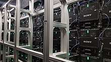
At CES 2017 Sony showcased the CLEDIS ™ (Crystal LED Integrated Structure) with a Crystal LED video wall approximately 32 by 9 feet with a resolution of 8000 x 2000 pixel. According to Sony, it is composed of single display modules measuring 17 7/8" (463.6mm) by 15 7/8" (403.2mm) each. The individual modules were not visible to the human eye. Due to the modular structure of the system theoretically, any resolution and size could be possible according to a Sony representative.[6]
References
- "Sony Intros 55-Inch Crystal LED Display Using 6 Million LEDs". Toms Hardware. Retrieved 19 January 2013.
- "40 Inch TVs". Monday, 5 November 2018
- "Sony Shows Off 55-Inch Crystal LED HDTV". PC World. Retrieved 19 January 2013.
- "Hands on: Sony Crystal LED TV prototype". TechRadar. Retrieved 19 January 2013.
- "Sony to choose between OLED and Crystal LED". TechRadar. Retrieved 19 January 2013.
- "The Future of Smart TVs". TechPrevue. Retrieved 28 April 2018.