Silicon on sapphire
Silicon on sapphire (SOS) is a hetero-epitaxial process for metal-oxide-semiconductor (MOS) integrated circuit (IC) manufacturing that consists of a thin layer (typically thinner than 0.6 µm) of silicon grown on a sapphire (Al2O3) wafer. SOS is part of the silicon-on-insulator (SOI) family of CMOS (complementary MOS) technologies.
Typically, high-purity artificially grown sapphire crystals are used. The silicon is usually deposited by the decomposition of silane gas (SiH4) on heated sapphire substrates. The advantage of sapphire is that it is an excellent electrical insulator, preventing stray currents caused by radiation from spreading to nearby circuit elements. SOS faced early challenges in commercial manufacturing because of difficulties in fabricating the very small transistors used in modern high-density applications. This is because the SOS process results in the formation of dislocations, twinning and stacking faults from crystal lattice disparities between the sapphire and silicon. Additionally, there is some aluminum, a p-type dopant, contamination from the substrate in the silicon closest to the interface.
History
In 1963, Harold M. Manasevit was the first to document epitaxial growth of silicon on sapphire while working at the Autonetics division of North American Aviation (now Boeing). In 1964, he published his findings with colleague William Simpson in the Journal of Applied Physics.[1] In 1965, C.W. Mueller and P.H. Robinson at RCA Laboratories fabricated a MOSFET (metal-oxide-semiconductor field-effect transistor) using the silicon-on-sapphire process.[2]
SOS was first used in aerospace and military applications because of its inherent resistance to radiation. More recently, patented advancements in SOS processing and design have been made by Peregrine Semiconductor, allowing SOS to be commercialized in high-volume for high-performance radio-frequency (RF) applications.
Circuits and systems

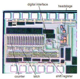
The advantages of the SOS technology allow research groups to fabricate a variety of SOS circuits and systems that benefit from the technology and advance the state-of-the-art in:
- analog-to-digital converters (a nano-Watts prototype was produced by Yale e-Lab)[4]
- monolithic digital isolation buffers[5]
- SOS-CMOS image sensor arrays (one of the first standard CMOS image sensor arrays capable of transducing light simultaneously from both sides of the die was produced by Yale e-Lab)[6]
- patch-clamp amplifiers[7]
- energy harvesting devices[8]
- three-dimensional (3D) integration with no galvanic connections
- charge pumps[9]
- temperature sensors[10]
Applications
Silicon on sapphire pressure transducer, pressure transmitter and temperature sensor diaphragms have been manufactured utilizing a patented process by Armen Sahagen since 1985.[11] Outstanding performance in high temperature environments helped propel this technology forward. This SOS technology has been licensed throughout the world. ESI Technology Ltd. in the UK have developed a wide range of pressure transducers and pressure transmitters that benefit from the outstanding features of silicon on sapphire.[12]
Peregrine Semiconductor has used SOS technology to develop RF integrated circuits (RFICs) including RF switches, digital step attenuators (DSAs), phase locked-loop (PLL) frequency synthesizers, prescalers, mixers/upconverters, and variable-gain amplifiers. These RFICs are designed for commercial RF applications such as mobile handsets and cellular infrastructure, broadband consumer and DTV, test and measurement, and industrial public safety, as well as rad-hard aerospace and defense markets.
Substrate analysis - SOS structure
The application of epitaxial growth of silicon on sapphire substrates for fabricating MOS devices involves a silicon purification process that mitigates crystal defects which result from a mismatch between sapphire and silicon lattices. For example, Peregrine Semiconductor's SP4T switch is formed on an SOS substrate where the final thickness of silicon is approximately 95 nm. Silicon is recessed in regions outside the polysilicon gate stack by poly oxidation and further recessed by the sidewall spacer formation process to a thickness of approximately 78 nm.
See also
References
- Manasevit, H. M.; Simpson, W. J. (1964). "Single-Crystal Silicon on a Sapphire Substrate". Journal of Applied Physics. 35: 1349. doi:10.1063/1.1713618.
- Mueller, C. W.; Robinson, P. H. (December 1964). "Grown-film silicon transistors on sapphire". Proceedings of the IEEE. 52 (12): 1487–1490. doi:10.1109/PROC.1964.3436.
- "Archived copy". Archived from the original on 2006-11-07. Retrieved 2006-11-12.CS1 maint: archived copy as title (link)
- "Archived copy" (PDF). Archived from the original (PDF) on 2011-09-27. Retrieved 2010-02-04.CS1 maint: archived copy as title (link)]"Archived copy" (PDF). Archived from the original (PDF) on 2011-09-27. Retrieved 2010-02-04.CS1 maint: archived copy as title (link)
- "Archived copy" (PDF). Archived from the original (PDF) on 2011-09-27. Retrieved 2010-02-04.CS1 maint: archived copy as title (link)
- "Archived copy" (PDF). Archived from the original (PDF) on 2011-09-27. Retrieved 2010-02-04.CS1 maint: archived copy as title (link)
- "Archived copy" (PDF). Archived from the original (PDF) on 2011-09-27. Retrieved 2010-02-04.CS1 maint: archived copy as title (link)
- "Archived copy" (PDF). Archived from the original (PDF) on 2011-09-27. Retrieved 2010-02-04.CS1 maint: archived copy as title (link)
- "Archived copy" (PDF). Archived from the original (PDF) on 2010-07-23. Retrieved 2010-02-04.CS1 maint: archived copy as title (link)
- "Archived copy" (PDF). Archived from the original (PDF) on 2010-07-23. Retrieved 2010-02-04.CS1 maint: archived copy as title (link)
- http://www.sensonetics.com
- http://www.esi-tec.com
Further reading
- Culurciello, Eugenio (2009). Silicon-on-Sapphire Circuits and Systems, Sensor and Biosensor interfaces. McGraw Hill.