Shallow trench isolation
Shallow trench isolation (STI), also known as box isolation technique, is an integrated circuit feature which prevents electric current leakage between adjacent semiconductor device components. STI is generally used on CMOS process technology nodes of 250 nanometers and smaller. Older CMOS technologies and non-MOS technologies commonly use isolation based on LOCOS.[1]

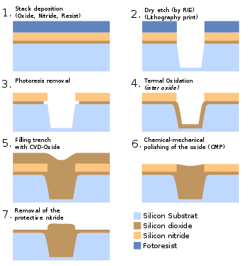
STI is created early during the semiconductor device fabrication process, before transistors are formed. The key steps of the STI process involve etching a pattern of trenches in the silicon, depositing one or more dielectric materials (such as silicon dioxide) to fill the trenches, and removing the excess dielectric using a technique such as chemical-mechanical planarization.
Certain semiconductor fabrication technologies also include deep trench isolation, a related feature often found in analog integrated circuits.
The effect of the trench edge has given rise to what has recently been termed the "reverse narrow channel effect"[2] or "inverse narrow width effect".[3] Basically, due to the electric field enhancement at the edge, it is easier to form a conducting channel (by inversion) at a lower voltage. The threshold voltage is effectively reduced for a narrower transistor width.[4][5] The main concern for electronic devices is the resulting subthreshold leakage current, which is substantially larger after the threshold voltage reduction.
Process flow
- Stack deposition (oxide + protective nitride)
- Lithography print
- Dry etch (Reactive-ion etching)
- Trench fill with oxide
- Chemical-mechanical polishing of the oxide
- Removal of the protective nitride
- Adjusting the oxide height to Si
See also
References
- Quirk, Michael & Julian Serda (2001). Semiconductor Manufacturing Technology: Instructor's Manual Archived September 28, 2007, at the Wayback Machine, p. 25.
- Jung, Jong-Wan; Kim, Jong-Min; Son, Jeong-Hwan; Lee, Youngjong (30 April 2000). "Dependence of Subthreshold Hump and Reverse Narrow Channel Effect on the Gate Length by Suppression of Transient Enhanced Diffusion at Trench Isolation Edge". Japanese Journal of Applied Physics. 39 (Part 1, No. 4B): 2136–2140. Bibcode:2000JaJAP..39.2136J. doi:10.1143/JJAP.39.2136.
- A. Chatterjee et al., IEDM 1996.(conference announcement) Chatterjee, A.; Esquivel, J.; Nag, S.; Ali, I.; Rogers, D.; Taylor, K.; Joyner, K.; Mason, M.; Mercer, D.; Amerasekera, A.; Houston, T.; Chen, I.-C. (1996), "A shallow trench isolation study for 0.25/0.18 μm CMOS technologies and beyond", 1996 Symposium on VLSI Technology. Digest of Technical Papers, pp. 156–157, doi:10.1109/VLSIT.1996.507831, ISBN 0-7803-3342-X
- Pretet, J; Ioannou, D; Subba, N; Cristoloveanu, S; Maszara, W; Raynaud, C (November 2002). "Narrow-channel effects and their impact on the static and floating-body characteristics of STI- and LOCOS-isolated SOI MOSFETs". Solid-State Electronics. 46 (11): 1699–1707. Bibcode:2002SSEle..46.1699P. doi:10.1016/S0038-1101(02)00147-8.
- Lee, Yung-Huei; Linton, Tom; Wu, Ken; Mielke, Neal (May 2001). "Effect of trench edge on pMOSFET reliability". Microelectronics Reliability. 41 (5): 689–696. doi:10.1016/S0026-2714(01)00002-6.