Rework (electronics)
Rework (or re-work) is the term for the refinishing operation or repair of an electronic printed circuit board (PCB) assembly, usually involving desoldering and re-soldering of surface-mounted electronic components (SMD). Mass processing techniques are not applicable to single device repair or replacement, and specialized manual techniques by expert personnel using appropriate equipment are required to replace defective components; area array packages such as ball grid array (BGA) devices particularly require expertise and appropriate tools. A hot air gun or hot air station is used to heat devices and melt solder, and specialised tools are used to pick up and position often tiny components.
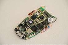
A rework station is a place to do this work—the tools and supplies for this work, typically on a workbench. Other kinds of rework require other tools.[1]
Reasons for rework
Rework is practiced in many kinds of manufacturing when defective products are found.[2]
For electronics, defects may include:
- Poor solder joints because of faulty assembly or thermal cycling.
- Solder bridges—unwanted drops of solder that connect points that should be isolated from each other.
- Faulty components.
- Engineering parts changes, upgrades, etc.
- Components broken due to natural wear, physical stress or excessive current.
- Components damaged due to liquid ingress, leading to corrosion, weak solder joints or physical damage.
Process
The rework may involve several components, which must be worked on one by one without damage to surrounding parts or the PCB itself. All parts not being worked on are protected from heat and damage. Thermal stress on the electronic assembly is kept as low as possible to prevent unnecessary contractions of the board which might cause immediate or future damage.
In the 21st century, almost all soldering is carried out with lead-free solder, both on manufactured assemblies and in rework, to avoid the health and environmental hazards of lead. Where this precaution is not necessary, tin-lead solder melts at a lower temperature and is easier to work with.
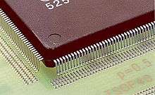
Heating a single SMD with a hot-air gun to melt all solder joints between it and the PCB is usually the first step, followed by removing the SMD while the solder is molten. The pad array on the conductor board should then be cleaned of old solder. It is quite easy to remove these residues by heating them to melting temperature. A soldering iron or hot air gun can be used with desoldering braid.
The precise placement of the new unit onto the prepared pad array requires skillful use of a highly accurate vision-alignment system with high resolution and magnification. The smaller the pitch and size of the components, the more precise working must be.
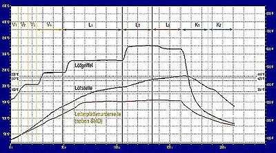
Finally the newly placed SMD is soldered onto the board. Reliable solder joints are facilitated by use of a solder profile which preheats the board, heats all the connections between the unit and the PCB to the melting temperature of the solder used, then properly cools them.
High quality demands or specific designs of SMDs require the precise application of solder paste before positioning and soldering the unit. The surface tension of the molten solder, which is on the board's solder pads, tends to pull the device into precise alignment with the pads if not initially positioned totally correctly.
Reflowing and reballing
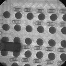

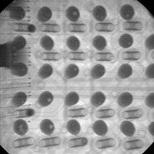
Ball grid arrays (BGA) and chip scale packages (CSA) present special difficulties for testing and rework, as they have many small, closely spaced pads on their underside which are connected to matching pads on the PCB. Connecting pins are not accessible from the top for testing, and cannot be desoldered without heating the whole device to the melting point of solder.
After fabrication of the BGA package, tiny balls of solder are glued to the pads on its underside; during assembly the balled package is placed on the PCB and heated to melt the solder and, all being well, to connect each pad on the device to its mate on the PCB without any extraneous solder bridging between adjacent pads. Bad connections produced during assembly can be detected and the assembly reworked (or scrapped). Imperfect connections of devices which are not themselves faulty, which work for a time and then fail, often triggered by thermal expansion and contraction at operating temperature, are not infrequent.
Assemblies which fail because of bad BGA connections can be repaired either by reflowing, or by removing the device and cleaning it of solder, reballing, and replacing. Devices can be recovered from scrapped assemblies for reuse in the same way.
Reflowing as a rework technique, similar to the manufacturing process of reflow soldering, involves dismantling the equipment to remove the faulty circuit board, pre-heating the whole board in an oven, heating the non-functioning component further to melt the solder, then cooling, following a carefully determined thermal profile, and reassembling, a process which is hoped will repair the bad connection without the need to remove and replace the component. This may or not resolve the problem; and there is a chance that the reflowed board will fail again after some time. For typical devices (PlayStation 3 and Xbox 360) one repair company estimates that the process, if there are no unexpected problems, takes about 80 minutes.[3] On a forum where professional repair people discuss reflowing of laptop computer graphics chips, different contributors cite success rates (no failure within 6 months) of between 60 and 90% for reflowing with professional equipment and techniques, in equipment whose value does not justify complete reballing.[4] Reflowing can be done non-professionally in a domestic oven[5] or with a heat gun.[6] While such methods can cure some problems, the outcome is likely to be less successful than is possible with accurate thermal profiling achieved by an experienced technician using professional equipment.
Reballing involves dismantling, heating the chip until it can be removed from the board, typically with a hot-air gun and vacuum pickup tool, removing the device, removing solder remaining on the device and board, putting new solder balls in place, replacing the original device if there was a poor connection, or using a new one, and heating the device or board to solder it in place. The new balls can be placed via several methods, including:
- Using a stencil for both the balls and the solder paste or flux,
- Using a BGA "preform" with embedded balls corresponding to the device pattern, or
- Using semiautomated or fully automated machinery.
For the PS3 and Xbox mentioned above, the time is about 120 minutes if all goes well.[3]
Chips are at risk of being damaged by the repeated heating and cooling of reballing, and manufacturers' warranties sometimes do not cover this case. Removing solder with solder wick subjects devices to thermal stress fewer times than using a flowing solder bath. In a test twenty devices were reballed, some several times. Two failed to function, but were restored to full functionality after reballing again. One was subjected to 17 thermal cycles without failing.
Results
Properly carried out rework restores the functionality of the reworked assembly, and its subsequent lifetime should not significantly be affected. Consequently, where the cost of reworking is less than the value of the assembly, it is widely used in all sectors of the electronic industry. Manufacturer and service providers of communications-technologies, entertainment- and consumer-devices, industrial commodities, automobiles, medical technology, aerospace and other high power electronics rework when necessary.
See also
References
- "Product Rework | Rework Process in Manufacturing". Lean Supply Solutions - Innovative Supply Chain Solutions. Retrieved 2020-06-02.
- Rasmussen, Patty. "Reduce Manufacturing Rework: Five Steps to Take". news.ewmfg.com. Retrieved 2019-02-23.
- Rework Analysis of PS3 YLOD & Xbox RROD: Reflow vs Reball
- badcaps.net forum: Laptop reflowing improving reliability?
- Repair VGA card by re-flowing solder on the board (using domestic oven)
- Sparkfun tutorials: Reflow skillet, July 2006