Photo–Dember effect
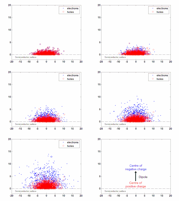
In semiconductor physics, the photo–Dember effect (named after its discoverer Harry Dember[1]) is the formation of a charge dipole in the vicinity of a semiconductor surface after ultra-fast photo-generation of charge carriers.[2] [3] [4] The dipole forms owing to the difference of mobilities (or diffusion constants) for holes and electrons which combined with the break of symmetry provided by the surface lead to an effective charge separation in the direction perpendicular to the surface. In an isolated sample, where the macroscopic flow of an electric current is prohibited, the fast carriers (often the electrons) are slowed and the slow carriers (often the holes) are accelerated by an electric field, called the Dember field.

One of the main applications of the photo–Dember effect is the generation of terahertz (THz) radiation pulses for terahertz time-domain spectroscopy. This effect is present in most semiconductors but it is particularly strong in narrow-gap semiconductors (mainly arsenides and antimonides) such as InAs[2][3] and InSb[4] owing to their high electron mobility. The photo–Dember terahertz emission should not be confused with the surface field emission, which occurs if the surface energy bands of a semiconductor fall between its valence and conduction bands, which produces a phenomenon known as Fermi level pinning, causing, at its time, band bending and consequently the formation of a depletion or accumulation layer close to the surface which contributes to the acceleration of charge carriers.[2] These two effects can contribute constructively or destructively for the dipole formation depending on the direction of the band-bending.
See also
References
- H. Dember (1931). "Über eine photoelektronische Kraft in Kupferoxydul-Kristallen (Photoelectric E.M.F. in Cuprous-Oxide Crystals)". Phys. Z. 32: 554.
- Johnston, M. B.; Whittaker, D. M.; Corchia, A.; Davies, A. G.; Linfield, E. H. (2002). "Simulation of terahertz generation at semiconductor surfaces". Physical Review B. 65 (16): 165301. Bibcode:2002PhRvB..65p5301J. doi:10.1103/PhysRevB.65.165301. ISSN 0163-1829.
- Dekorsy, T.; Auer, H.; Bakker, H. J.; Roskos, H. G.; Kurz, H. (1996). "THz electromagnetic emission by coherent infrared-active phonons" (PDF). Physical Review B. 53 (7): 4005–4014. Bibcode:1996PhRvB..53.4005D. doi:10.1103/PhysRevB.53.4005. ISSN 0163-1829. PMID 9983955.
- Kono, S.; Gu, P.; Tani, M.; Sakai, K. (2000). "Temperature dependence of terahertz radiation from n-type InSb and n-type InAs surfaces". Applied Physics B. 71 (6): 901–904. doi:10.1007/s003400000455. ISSN 0946-2171.