Pass transistor logic
In electronics, pass transistor logic (PTL) describes several logic families used in the design of integrated circuits. It reduces the count of transistors used to make different logic gates, by eliminating redundant transistors. Transistors are used as switches to pass logic levels between nodes of a circuit, instead of as switches connected directly to supply voltages.[1] This reduces the number of active devices, but has the disadvantage that the difference of the voltage between high and low logic levels decreases at each stage. Each transistor in series is less saturated at its output than at its input.[2] If several devices are chained in series in a logic path, a conventionally constructed gate may be required to restore the signal voltage to the full value. By contrast, conventional CMOS logic switches transistors so the output connects to one of the power supply rails, so logic voltage levels in a sequential chain do not decrease. Simulation of circuits may be required to ensure adequate performance.
Applications
.svg.png)

Pass transistor logic often uses fewer transistors, runs faster, and requires less power than the same function implemented with the same transistors in fully complementary CMOS logic.[3]
XOR has the worst-case Karnaugh map—if implemented from simple gates, it requires more transistors than any other function. The designers of the Z80 and many other chips saved a few transistors by implementing the XOR using pass-transistor logic rather than simple gates.[4]
Basic principles of pass transistor circuits
The pass transistor is driven by a periodic clock signal and acts as an access switch to either charge up or charge down the parasitic capacitance Cx, depending on the input signal Vin. Thus there is two possible operations , when the clock signal is active (CK = 1) are the logic "1" transfer (charging up the capacitance Cx to a logic-high level) and the logic "0" transfer (charging down the capacitance Cx to a logic-low level). In either case, the output of the depletion load nMOS inverter obviously assumes a logic-low or a logic-high level, depending upon the voltage Vx.
Complementary pass transistor logic
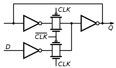
Some authors use the term "complementary pass transistor logic" to indicate a style of implementing logic gates that uses transmission gates composed of both NMOS and PMOS pass transistors.[5]
Other authors use the term "complementary pass transistor logic" (CPL) to indicate a style of implementing logic gates where each gate consists of a NMOS-only pass transistor network, followed by a CMOS output inverter.[6][7][8]
Other authors use the term "complementary pass transistor logic" (CPL) to indicate a style of implementing logic gates using dual-rail encoding. Every CPL gate has two output wires, both the positive signal and the complementary signal, eliminating the need for inverters.[9][10][11]
Complementary pass transistor logic or "Differential pass transistor logic" refers to a logic family which is designed for certain advantage. It is common to use this logic family for multiplexers and latches.
CPL uses series transistors to select between possible inverted output values of the logic, the output of which drives an inverter The CMOS transmission gates consist of nMOS and pMOS transistor connected in parallel.
Other forms
Static and dynamic types of pass transistor logic exist, with differing properties with respect to speed, power and low-voltage operation.[12] As integrated circuit supply voltages decrease, the disadvantages of pass transistor logic become more significant; the threshold voltage of transistors becomes large compared to the supply voltage, severely limiting the number of sequential stages. Because complementary inputs are often required to control pass transistors, additional logic stages are required.
References
- Jaume Segura, Charles F. Hawkins CMOS electronics: how it works, how it fails, Wiley-IEEE, 2004 ISBN 0-471-47669-2, page 132
- Clive Maxfield Bebop to the boolean boogie: an unconventional guide to electronicsNewnes, 2008 ISBN 1-85617-507-3, pp. 423-426
- Norimitsu Sako. "Patent US7171636: Pass-transistor logic circuit and a method of designing thereof". 'It is known in the art to employ a "pass-transistor logic circuit" to reduce a number of elements and power consumption, and to improve operating speed.'
- Ken Shirriff. "Reverse-engineering the Z-80: the silicon for two interesting gates explained". 2013.
- Gary K. Yeap. "Practical Low Power Digital VLSI Design". 2012. p. 197.
- Vojin G. Oklobdzija. "Digital Design and Fabrication". p. 2-39.
- Yano, Kuniaki; Yamanaka, Toshiaki Yamanaka; Nishida, Takeshi; Saito, Mitsuo; Shimohigashi, Katsuhiro; Shimizu, Atsushi (1990). "A 3.8-ns CMOS 16x16-b multiplier using complementary pass-transistor logic". IEEE Journal of Solid-State Circuits. 25 (2): 388–395. doi:10.1109/4.52161.
- Reynders, Nele; Dehaene, Wim (2015). Written at Heverlee, Belgium. Ultra-Low-Voltage Design of Energy-Efficient Digital Circuits. Analog Circuits And Signal Processing (ACSP) (1 ed.). Cham, Switzerland: Springer International Publishing AG Switzerland. doi:10.1007/978-3-319-16136-5. ISBN 978-3-319-16135-8. ISSN 1872-082X. LCCN 2015935431.
- Wai-Kai Chen. "Logic Design". 2003. p. 15-7.
- Vojin G. Oklobdzija. "The Computer Engineering Handbook". 2001. p. 2-23 to 2-24.
- Ajit Pal. "Low-Power VLSI Circuits and Systems". p. 109 to 110.
- Cornelius T. Leondes Digital signal processing systems: implementation techniques Elsevier, 1995 ISBN 0-12-012768-7 page 2
Further reading
- Weste and Harris, CMOS VLSI Design, Third Edition (ISBN 0-321-14901-7; ISBN 0-321-26977-2 (international edition))
- Douglas A. Pucknell and Kamran Eshraghian, Basic VLSI Design, Third Edition (ISBN 978-81-203-0986-9 (Indian Edition))