Nanostructured film
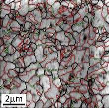
A nanostructured film is a film resulting from engineering of nanoscale features, such as dislocations, grain boundaries, defects, or twinning. In contrast to other nanostructures, such as nanoparticles, the film itself may be up to several microns thick, but possesses a large concentration of nanoscale features homogeneously distributed throughout the film. Like other nanomaterials, nanostructured films have sparked much interest as they possess unique properties not found in bulk, non-nanostructured material of the same composition. In particular, nanostructured films have been the subject of recent research due to their superior mechanical properties, including strength, hardness, and corrosion resistance compared to regular films of the same material.[1] Examples of nanostructured films include those produced by grain boundary engineering, such as nano-twinned ultra-fine grain copper, or dual phase nanostructuring, such as crystalline metal and amorphous metallic glass nanocomposites.[2]

Synthesis and characterization
Nanostructured films are commonly created using magnetron sputtering from an appropriate target material.[3] Films can be elemental in nature, formed by sputtering from a pure metal target such as copper, or composed of compound materials. Varying parameters such as the sputtering rate, substrate temperature, and sputtering interrupts allow the creation of films with a variety of different nanostructured elements. Control over nano-twinning, tailoring of specific types of grain boundaries, and restricting the movement and propagation of dislocations have been demonstrated using films produced via magnetron sputtering.[4]
Methods used to characterize nanostructured films include transmission electron microscopy, scanning electron microscopy, electron backscatter diffraction, focused ion beam milling, and nanoindentation.[1][2] These techniques are used as they allow imaging of nanoscale structures, including dislocations, twinning, grain boundaries, film morphology, and atomic structure.
Material properties
Nanostructured films are of interest due to their superior mechanical and physical properties compared to their normal equivalent. Elemental nanostructured films composed of pure copper were found to possess good thermal stability due to the nano-twinned film possessing a higher fraction of grain boundaries.[1] In addition to possessing higher thermal stability, copper films that were highly nano-twinned were found to have a better corrosion resistance than copper films with a low concentration of nano-twins.[5] Control of the fraction of grains in a material with nano-twins present has great potential for less expensive alloys and coatings with a good degree of corrosion resistance.
Compound nanostructured films composed of crystalline MgCu2 cores encapsulated by amorphous glassy shells of the same material were shown to possess a near-ideal mechanical strength.[2] The crystalline MgCu2 cores, typically less than 10 nm in size, were found to substantially strengthen the material by restricting the movement of dislocations and grains. The cores were also found to contribute to overall material strength by restricting the movement of shear bands in the material. This nanostructured film differs from both crystalline metals and amorphous metallic glasses, both of which exhibit behaviors such as the reverse Hall-Petch and shear-band softening effects that prevent them from reaching ideal strength values.[2]
Applications
Nanostructured films with superior mechanical properties allow previously unusable materials to be utilized in new applications, enabling advances fields where coatings are heavily utilized, such as aerospace, energy, and other engineering fields.[6] Production scalability of nanostructured films has already been demonstrated, and the ubiquity of sputtering techniques in industry is predicted to facilitate the incorporation of nanostructured films into existing applications.[4]
See also
References
- Zhao, Yifu; Furnish, Timothy Allen; Kassner, Michael Ernest; Hodge, Andrea Maria (2012). "Thermal stability of highly nanotwinned copper: The role of grain boundaries and texture". Journal of Materials Research. 27 (24): 3049–3057. doi:10.1557/jmr.2012.376. ISSN 0884-2914.
- Wu, Ge; Chan, Ka-Cheung; Zhu, Linli; Sun, Ligang; Lu, Jian (2017). "Dual-phase nanostructuring as a route to high-strength magnesium alloys". Nature. 545 (7652): 80–83. doi:10.1038/nature21691. PMID 28379942.
- Polyakov, Mikhail N.; Chookajorn, Tongjai; Mecklenburg, Matthew; Schuh, Christopher A.; Hodge, Andrea M. (2016-04-15). "Sputtered Hf–Ti nanostructures: A segregation and high-temperature stability study". Acta Materialia. 108: 8–16. doi:10.1016/j.actamat.2016.01.073.
- Hodge, A. M.; Wang, Y. M.; Barbee Jr., T. W. (2006-08-15). "Large-scale production of nano-twinned, ultrafine-grained copper". Materials Science and Engineering: A. 429 (1–2): 272–276. doi:10.1016/j.msea.2006.05.109.
- Zhao, Y.; Cheng, I. C.; Kassner, M. E.; Hodge, A. M. (April 2014). "The effect of nanotwins on the corrosion behavior of copper". Acta Materialia. 67: 181–188. doi:10.1016/j.actamat.2013.12.030.
- Lu, L.; Chen, X.; Huang, X.; Lu, K. (2009-01-30). "Revealing the Maximum Strength in Nanotwinned Copper". Science. 323 (5914): 607–610. doi:10.1126/science.1167641. ISSN 0036-8075. PMID 19179523.