Monocrystalline silicon
Monocrystalline silicon, more often called single-crystal silicon, in short mono c-Si or mono-Si, is the base material for silicon-based discrete components and integrated circuits used in virtually all modern electronic equipment. Mono-Si also serves as a photovoltaic, light-absorbing material in the manufacture of solar cells.
It consists of silicon in which the crystal lattice of the entire solid is continuous, unbroken to its edges, and free of any grain boundaries. Mono-Si can be prepared as an intrinsic semiconductor that consists only of exceedingly pure silicon, or it can be doped by the addition of other elements such as boron or phosphorus to make p-type or n-type silicon.[1] Due to its semiconducting properties, single-crystal silicon is perhaps the most important technological material of the last few decades—the "silicon era",[2] because its availability at an affordable cost has been essential for the development of the electronic devices on which the present-day electronics and IT revolution is based.
Monocrystalline silicon differs from other allotropic forms, such as non-crystalline amorphous silicon—used in thin-film solar cells—and polycrystalline silicon, which consists of small crystals known as crystallites.
Production
Monocrystalline silicon is generally created by one of several methods that involve melting high-purity, semiconductor-grade silicon (only a few parts per million of impurities) and the use of a seed to initiate the formation of a continuous single crystal. This process is normally performed in an inert atmosphere, such as argon, and in an inert crucible, such as quartz, to avoid impurities that would affect the crystal uniformity.
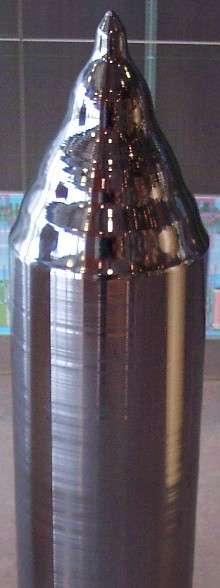
The most common production technique is the Czochralski method, which dips a precisely oriented rod-mounted seed crystal into the molten silicon. The rod is then slowly pulled upwards and rotated simultaneously, allowing the pulled material to solidify into a monocrystalline cylindrical ingot up to 2 meters in length and weighing several hundred kilograms. Magnetic fields may also be applied to control and suppress turbulent flow, further improving the uniformity of the crystallization.[3] Other methods are zone melting, which passes a polycrystalline silicon rod through a radiofrequency heating coil that creates a localized molten zone, from which a seed crystal ingot grows, and Bridgman techniques, which move the crucible through a temperature gradient to cool it from the end of the container containing the seed.[4] The solidified ingots are then sliced into thin wafers during a process called wafering. After post-wafering processing, the wafers are ready for use in fabrication.
Compared to the casting of polycrystalline ingots, the production of monocrystalline silicon is very slow and expensive. However, the demand for mono-Si continues to rise due to the superior electronic properties—the lack of grain boundaries allows better charge carrier flow and prevents electron recombination[5]—allowing improved performance of integrated circuits and photovoltaics.
In electronics
The primary application of monocrystalline silicon is in the production of discrete components and integrated circuits. Ingots made by the Czochralski method are sliced into wafers about 0.75 mm thick and polished to obtain a regular, flat substrate, onto which microelectronic devices are built through various microfabrication processes, such as doping or ion implantation, etching, deposition of various materials, and photolithographic patterning.
A single continuous crystal is critical for electronics, since grain boundaries, impurities, and crystallographic defects can significantly impact the local electronic properties of the material, which in turn affects the functionality, performance, and reliability of semiconductor devices by interfering with their proper operation. For example, without crystalline perfection, it would be virtually impossible to build very large-scale integration (VLSI) devices, in which billions[6] of transistor-based circuits, all of which must function reliably, are combined into a single chip to form a microprocessor. As such, the electronics industry has invested heavily in facilities to produce large single crystals of silicon.
In solar cells
Monocrystalline silicon is also used for high-performance photovoltaic (PV) devices. Since there are less stringent demands on structural imperfections compared to microelectronics applications, lower-quality solar-grade silicon (Sog-Si) is often used for solar cells. Despite this, the monocrystalline-silicon photovoltaic industry has benefitted greatly from the development of faster mono-Si production methods for the electronics industry.
Market share
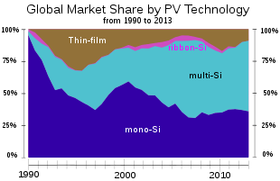
Being the second most common form of PV technology, monocrystalline silicon is ranked behind only its sister, polycrystalline silicon. Due to the significantly higher production rate and steadily decreasing costs of poly-silicon, the market share of mono-Si has been decreasing: in 2013, monocrystalline solar cells had a market share of 36%, which translated into the production of 12.6 GW of photovoltaic capacity,[7] but the market share had dropped below 25% by 2016. Despite the lowered market share, the equivalent mono-Si PV capacity produced in 2016 was 20.2 GW, indicating a significant increase in the overall production of photovoltaic technologies.[8]
Efficiency
With a recorded single-junction cell lab efficiency of 26.7%, monocrystalline silicon has the highest confirmed conversion efficiency out of all commercial PV technologies, ahead of poly-Si (22.3%) and established thin-film technologies, such as CIGS cells (21.7%), CdTe cells (21.0%), and a-Si cells (10.2%). Solar module efficiencies for mono-Si—which are always lower than those of their corresponding cells—finally crossed the 20% mark for in 2012 and hit 24.4% in 2016.[9] The high efficiency is largely attributable to the lack of recombination sites in the single crystal and better absorption of photons due to its black color, as compared to the characteristic blue hue of poly-silicon. Since they are more expensive than their polycrystalline counterparts, mono-Si cells are useful for applications where the main considerations are limitations on weight or available area, such as in spacecraft or satellites powered by solar energy, where efficiency can be further improved through combination with other technologies, such as multi-layer solar cells.
Manufacturing
Besides the low production rate, there are also concerns over wasted material in the manufacturing process. Creating space-efficient solar panels requires cutting the circular wafers (a product of the cylindrical ingots formed through the Czochralski process) into octagonal cells that can be packed closely together. The leftover material is not used to create PV cells and is either discarded or recycled by going back to ingot production for melting. Furthermore, even though mono-Si cells can absorb the majority of photons within 20 μm of the incident surface, limitations on the ingot sawing process mean commercial wafer thickness are generally around 200 μm. However, advances in technology are expected to reduce wafer thicknesses to 140 μm by 2026.[10]
Other manufacturing methods are being researched, such as direct wafer epitaxial growth, which involves growing gaseous layers on reusable silicon substrates. Newer processes may allow growth of square crystals that can then be processed into thinner wafers without compromising quality or efficiency, thereby eliminating the waste from traditional ingot sawing and cutting methods.[11]
Appearance
| Wikimedia Commons has media related to Monocrystalline silicon solar cells. |
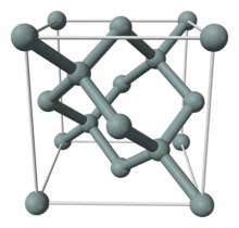 The crystal structure of silicon forms a diamond cubic
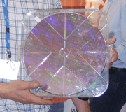
 Solar panel made of octagonal monocrystalline silicon cells
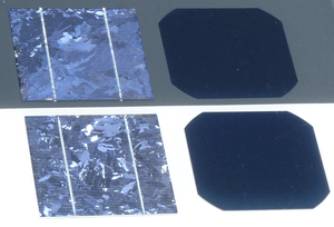 Comparison of solar cells: poly-Si (left) and mono-Si (right)
References
- Monkowski, J. R.; Bloem, J.; Giling, L. J.; Graef, M. W. M. (1979). "Comparison of dopant incorporation into polycrystalline and monocrystalline silicon". Appl. Phys. Lett. 35 (5): 410–412. doi:10.1063/1.91143.
- W.Heywang, K.H.Zaininger, Silicon: the semiconductor material, in Silicon: evolution and future of a technology, P.Siffert, E.F.Krimmel eds., Springer Verlag, 2004.
- Wang, C.; Zhang, H.; Wang, T. H.; Ciszek, T. F. (2003). "A continuous Czochralski silicon crystal growth system". Journal of Crystal Growth. 250 (1–2): 209–214. doi:10.1016/s0022-0248(02)02241-8.
- Capper, Peter; Rudolph, Peter (2010). Crystal growth technology: semiconductors and dielectrics. Weinheim: Wiley-VCH. ISBN 9783527325931. OCLC 663434790.
- Wenham, S. R.; Green, M. A.; Watt, M. E.; Corkish R. (2007). Applied photovoltaics (2nd ed.). London: Earthscan. ISBN 9781844074013. OCLC 122927906.
- Peter Clarke, Intel enters billion-transistor processor era, EE Times, 14 October 2005.
- Photovoltaics Report, Fraunhofer ISE, July 28, 2014.
- Photovoltaics Report, Fraunhofer ISE, February 26, 2018.
- Green, Martin A.; Hishikawa, Yoshihiro; Dunlop, Ewan D.; Levi, Dean H.; Hohl-Ebinger, Jochen; Ho-Baillie, Anita W. Y. (2018-01-01). "Solar cell efficiency tables (version 51)". Progress in Photovoltaics: Research and Applications. 26 (1): 3–12. doi:10.1002/pip.2978. ISSN 1099-159X.
- Solar Industry Technology Report 2015–2016, Canadian Solar, October 2016.
- Scanlon, Bill (August 27, 2014). "Crystal Solar and NREL Team Up to Cut Costs". NREL. Retrieved 2018-03-01.
