Reflection high-energy electron diffraction
Reflection high-energy electron diffraction (RHEED) is a technique used to characterize the surface of crystalline materials. RHEED systems gather information only from the surface layer of the sample, which distinguishes RHEED from other materials characterization methods that also rely on diffraction of high-energy electrons. Transmission electron microscopy, another common electron diffraction method samples the bulk of the sample due to the geometry of the system. Low-energy electron diffraction (LEED) is also surface sensitive, but LEED achieves surface sensitivity through the use of low energy electrons.
Introduction
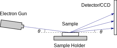
A RHEED system requires an electron source (gun), photoluminescent detector screen and a sample with a clean surface, although modern RHEED systems have additional parts to optimize the technique.[1][2] The electron gun generates a beam of electrons which strike the sample at a very small angle relative to the sample surface. Incident electrons diffract from atoms at the surface of the sample, and a small fraction of the diffracted electrons interfere constructively at specific angles and form regular patterns on the detector. The electrons interfere according to the position of atoms on the sample surface, so the diffraction pattern at the detector is a function of the sample surface. Figure 1 shows the most basic setup of a RHEED system.
Surface diffraction
In the RHEED setup, only atoms at the sample surface contribute to the RHEED pattern.[3] The glancing angle of incident electrons allows them to escape the bulk of the sample and to reach the detector. Atoms at the sample surface diffract (scatter) the incident electrons due to the wavelike properties of electrons.
The diffracted electrons interfere constructively at specific angles according to the crystal structure and spacing of the atoms at the sample surface and the wavelength of the incident electrons. Some of the electron waves created by constructive interference collide with the detector, creating specific diffraction patterns according to the surface features of the sample. Users characterize the crystallography of the sample surface through analysis of the diffraction patterns. Figure 2 shows a RHEED pattern. Video 1 depicts a metrology instrument recording the RHEED intensity oscillations and deposition rate for process control and analysis.
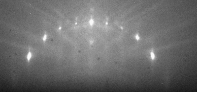
Two types of diffraction contribute to RHEED patterns. Some incident electrons undergo a single, elastic scattering event at the crystal surface, a process termed kinematic scattering.[1] Dynamic scattering occurs when electrons undergo multiple diffraction events in the crystal and lose some of their energy due to interactions with the sample.[1] Users extract non-qualitative data from the kinematically diffracted electrons. These electrons account for the high intensity spots or rings common to RHEED patterns. RHEED users also analyze dynamically scattered electrons with complex techniques and models to gather quantitative information from RHEED patterns.[3]
Kinematic scattering analysis
RHEED users construct Ewald's spheres to find the crystallographic properties of the sample surface. Ewald's spheres show the allowed diffraction conditions for kinematically scattered electrons in a given RHEED setup. The diffraction pattern at the screen relates to the Ewald's sphere geometry, so RHEED users can directly calculate the reciprocal lattice of the sample with a RHEED pattern, the energy of the incident electrons and the distance from the detector to the sample. The user must relate the geometry and spacing of the spots of a perfect pattern to the Ewald's sphere in order to determine the reciprocal lattice of the sample surface.
The Ewald's sphere analysis is similar to that for bulk crystals, however the reciprocal lattice for the sample differs from that for a 3D material due to the surface sensitivity of the RHEED process. The reciprocal lattices of bulk crystals consist of a set of points in 3D space. However, only the first few layers of the material contribute to the diffraction in RHEED, so there are no diffraction conditions in the dimension perpendicular to the sample surface. Due to the lack of a third diffracting condition, the reciprocal lattice of a crystal surface is a series of infinite rods extending perpendicular to the sample's surface.[4] These rods originate at the conventional 2D reciprocal lattice points of the sample's surface.
The Ewald's sphere is centered on the sample surface with a radius equal to the reciprocal of the wavelength of the incident electrons. The relationship is given by
where λ is the wavelength of incident electrons.
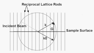
Diffraction conditions are satisfied where the rods of reciprocal lattice intersect the Ewald's sphere. Therefore, the magnitude of a vector from the origin of the Ewald's sphere to the intersection of any reciprocal lattice rods is equal in magnitude to that of the incident beam. Equation 2 shows this relationship.
(2)
Where: k0=incident electron wave vector
ki=electron wave vector at any intersection of reciprocal lattice with Ewald's sphere
An arbitrary vector, G, defines the reciprocal lattice vector between the ends of any two k vectors. Vector G is useful for finding distance between arbitrary planes in the crystal. Vector G is calculated using Equation 3.
(3)
Figure 3 shows the construction of the Ewald's sphere and provides examples of the G, k and k0 vectors.
Many of the reciprocal lattice rods meet the diffraction condition, however the RHEED system is designed such that only the low orders of diffraction are incident on the detector. The RHEED pattern at the detector is a projection only of the k vectors that are within the angular range that contains the detector. The size and position of the detector determine which of the diffracted electrons are within the angular range that reaches the detector, so the geometry of the RHEED pattern can be related back to the geometry of the reciprocal lattice of the sample surface through use of trigonometric relations and the distance from the sample to detector.
The k vectors are labeled such that the k vector that forms the smallest angle with the sample surface is called 0th order beam.[3] The 0th order beam is also known as the specular beam. Each successive intersection of a rod and the sphere further from the sample surface is labeled as a higher order reflection. The center of the Ewald's sphere is positioned such that the specular beam forms the same angle with the substrate as the incident electron beam. The specular point has the greatest intensity on a RHEED pattern and is labeled as the (00) point by convention.[3] The other points on the RHEED pattern are indexed according to the reflection order they project.
The radius of the Ewald's sphere is much larger than the spacing between reciprocal lattice rods because the incident beam has a very short wavelength due to its high-energy electrons. Rows of reciprocal lattice rods actually intersect the Ewald's sphere as an approximate plane because identical rows of parallel reciprocal lattice rods sit directly in front and behind the single row shown.[1] Figure 3 shows a cross sectional view of a single row of reciprocal lattice rods filling of the diffraction conditions. The reciprocal lattice rods in Figure 3 show the end on view of these planes, which are perpendicular to the computer screen in the figure.
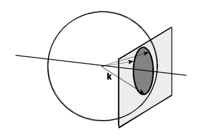
The intersections of these effective planes with the Ewald's sphere forms circles, called Laue circles. The RHEED pattern is a collection of points on the perimeters of concentric Laue circles around the center point. However, interference effects between the diffracted electrons still yield strong intensities at single points on each Laue circle. Figure 4 shows the intersection of one of these planes with the Ewald's Sphere.
The azimuthal angle affects the geometry and intensity of RHEED patterns.[4] The azimuthal angle is the angle at which the incident electrons intersect the ordered crystal lattice on the surface of the sample. Most RHEED systems are equipped with a sample holder that can rotate the crystal around an axis perpendicular to the sample surface. RHEED users rotate the sample to optimize the intensity profiles of patterns. Users generally index at least 2 RHEED scans at different azimuth angles for reliable characterization of the crystal's surface structure.[4] Figure 5 shows a schematic diagram of an electron beam incident on the sample at different azimuth angles.

Users sometimes rotate the sample around an axis perpendicular to the sampling surface during RHEED experiments to create a RHEED pattern called the azimuthal plot.[4] Rotating the sample changes the intensity of the diffracted beams due to their dependence on the azimuth angle.[5] RHEED specialists characterize film morphologies by measuring the changes in beam intensity and comparing these changes to theoretical calculations, which can effectively model the dependence of the intensity of diffracted beams on the azimuth angle.[5]
Dynamic scattering analysis
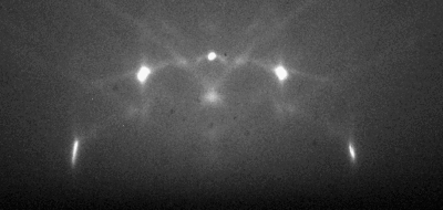
The dynamically, or inelastically, scattered electrons provide several types of information about the sample as well. The brightness or intensity at a point on the detector depends on dynamic scattering, so all analysis involving the intensity must account for dynamic scattering.[1][3] Some inelastically scattered electrons penetrate the bulk crystal and fulfill Bragg diffraction conditions. These inelastically scattered electrons can reach the detector to yield kikuchi diffraction patterns, which are useful for calculating diffraction conditions.[3] Kikuchi patterns are characterized by lines connecting the intense diffraction points on a RHEED pattern. Figure 6 shows a RHEED pattern with visible Kikuchi lines.
RHEED system requirements
Electron gun
The electron gun is one of the most important piece of equipment in a RHEED system.[1] The gun limits the resolution and testing limits of the system. Tungsten filaments are the primary electron source for the electron gun of most RHEED systems due to the low work function of tungsten. In the typical setup, the tungsten filament is the cathode and a positively biased anode draws electrons from the tip of the tungsten filament.[1]
The magnitude of the anode bias determines the energy of the incident electrons. The optimal anode bias is dependent upon the type of information desired. At large incident angles, electrons with high energy can penetrate the surface of the sample and degrade the surface sensitivity of the instrument.[1] However, the dimensions of the Laue zones are proportional to the inverse square of the electron energy meaning that more information is recorded at the detector at higher incident electron energies.[1] For general surface characterization, the electron gun is operated the range of 10-30 keV.[3]
In a typical RHEED setup, one magnetic and one electric field focus the incident beam of electrons.[1] A negatively biased Wehnelt electrode positioned between the cathode filament and anode applies a small electric field, which focuses the electrons as they pass through the anode. An adjustable magnetic lens focuses the electrons onto the sample surface after they pass through the anode. A typical RHEED source has a focal length around 50 cm.[3] The beam is focused to the smallest possible point at the detector rather than the sample surface so that the diffraction pattern has the best resolution.[1]
Phosphor screens that exhibit photoluminescence are widely used as detectors. These detectors emit green light from areas where electrons hit their surface and are common to TEM as well. The detector screen is useful for aligning the pattern to an optimal position and intensity. CCD cameras capture the patterns to allow for digital analysis.
Sample surface
The sample surface must be extremely clean for effective RHEED experiments. Contaminants on the sample surface interfere with the electron beam and degrade the quality of the RHEED pattern. RHEED users employ two main techniques to create clean sample surfaces. Small samples can be cleaved in the vacuum chamber prior to RHEED analysis.[6] The newly exposed, cleaved surface is analyzed. Large samples, or those that are not able to be cleaved prior to RHEED analysis can be coated with a passive oxide layer prior to analysis.[6] Subsequent heat treatment under the vacuum of the RHEED chamber removes the oxide layer and exposes the clean sample surface.
Vacuum requirements
Because gas molecules diffract electrons and affect the quality of the electron gun, RHEED experiments are performed under vacuum. The RHEED system must operate at a pressure low enough to prevent significant scattering of the electron beams by gas molecules in the chamber. At electron energies of 10keV, a chamber pressure of 10−5 mbar or lower is necessary to prevent significant scattering of electrons by the background gas.[6] In practice, RHEED systems are operated under ultra high vacuums. The chamber pressure is minimized as much as possible in order to optimize the process. The vacuum conditions limit the types of materials and processes that can be monitored in situ with RHEED.
RHEED patterns of real surfaces
Previous analysis focused only on diffraction from a perfectly flat surface of a crystal surface. However, non-flat surfaces add additional diffraction conditions to RHEED analysis.
Streaked or elongated spots are common to RHEED patterns. As Fig 3 shows, the reciprocal lattice rods with the lowest orders intersect the Ewald sphere at very small angles, so the intersection between the rods and sphere is not a singular point if the sphere and rods have thickness. The incident electron beam diverges and electrons in the beam have a range of energies, so in practice, the Ewald sphere is not infinitely thin as it is theoretically modeled. The reciprocal lattice rods have a finite thickness as well, with their diameters dependent on the quality of the sample surface. Streaks appear in the place of perfect points when broadened rods intersect the Ewald sphere. Diffraction conditions are fulfilled over the entire intersection of the rods with the sphere, yielding elongated points or ‘streaks’ along the vertical axis of the RHEED pattern. In real cases, streaky RHEED patterns indicate a flat sample surface while the broadening of the streaks indicate small area of coherence on the surface.
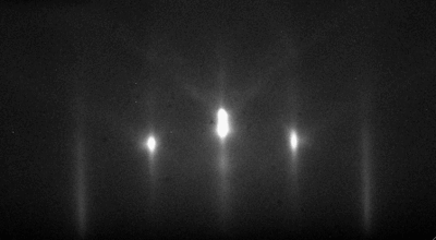
Surface features and polycrystalline surfaces add complexity or change RHEED patterns from those from perfectly flat surfaces. Growing films, nucleating particles, crystal twinning, grains of varying size and adsorbed species add complicated diffraction conditions to those of a perfect surface.[7][8] Superimposed patterns of the substrate and heterogeneous materials, complex interference patterns and degradation of the resolution are characteristic of complex surfaces or those partially covered with heterogeneous materials.
Specialized RHEED techniques
Film growth
RHEED is an extremely popular technique for monitoring the growth of thin films. In particular, RHEED is well suited for use with molecular beam epitaxy (MBE), a process used to form high quality, ultrapure thin films under ultrahigh vacuum growth conditions.[9] The intensities of individual spots on the RHEED pattern fluctuate in a periodic manner as a result of the relative surface coverage of the growing thin film. Figure 8 shows an example of the intensity fluctuating at a single RHEED point during MBE growth.
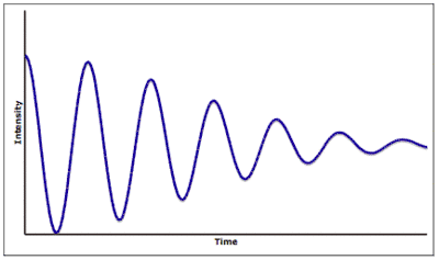
Each full period corresponds to formation of a single atomic layer thin film. The oscillation period is highly dependent on the material system, electron energy and incident angle, so researchers obtain empirical data to correlate the intensity oscillations and film coverage before using RHEED for monitoring film growth.[6]
Video 1 depicts a metrology instrument recording the RHEED intensity oscillations and deposition rate for process control and analysis.
RHEED-TRAXS
Reflection high energy electron diffraction - total reflection angle X-ray spectroscopy is a technique for monitoring the chemical composition of crystals.[10] RHEED-TRAXS analyzes X-ray spectral lines emitted from a crystal as a result of electrons from a RHEED gun colliding with the surface.
RHEED-TRAXS is preferential to X-ray microanalysis (XMA)(such as EDS and WDS) because the incidence angle of the electrons on the surface is very small, typically less than 5°. As a result, the electrons do not penetrate deeply into the crystal, meaning the X-ray emission is restricted to the top of the crystal, allowing for real-time, in-situ monitoring of surface stoichiometry.
The experimental setup is fairly simple. Electrons are fired onto a sample causing X-ray emission. These X-rays are then detected using a silicon-lithium Si-Li crystal placed behind beryllium windows, used to maintain vacuum.
MCP-RHEED
MCP-RHEED is a system in which an electron beam is amplified by a micro-channel plate (MCP). This system consists of an electron gun and an MCP equipped with a fluorescent screen opposite to the electron gun. Because of the amplification, the intensity of the electron beam can be decreased by several orders of magnitude and the damage to the samples is diminished. This method is used to observe the growth of insulator crystals such as organic films and alkali halide films, which are easily damaged by electron beams.[11]
References
- Ichimiya A & Cohen P I (2004). Reflection High Energy Electron Diffraction. Cambridge University Press: Cambridge, UK. pp. 1, 13, 16, 98, 130, 161. ISBN 0-521-45373-9.
- Horio Y; Hashimoto Y & Ichimaya A (1996). "A new type of RHEED apparatus equipped with an energy filter". Appl. Surf. Sci. 100: 292–6. Bibcode:1996ApSS..100..292H. doi:10.1016/0169-4332(96)00229-2.
- Braun W (1999). Applied RHEED: Reflection High-Energy Electron Diffraction During Crystal Growth. Springer-Verlag: Berlin. pp. 14–17, 25, 75. ISBN 3-540-65199-3.
- Oura K; Lifshits V G; Saranin A A; Zotov A V & Katayama M (2001). Surface Science: An Introduction. Springer-Verlag: Berlin. pp. 59–65. ISBN 3-540-00545-5.
- Mitura Z & Maksym P A (1993). "Analysis of reflection high energy electron diffraction azimuthal plots". Phys. Rev. Lett. 70 (19): 2904–2907. Bibcode:1993PhRvL..70.2904M. doi:10.1103/PhysRevLett.70.2904. PMID 10053683.
- Dobson P J (1988). Howie A; Valdre U (eds.). Surface and Interface Characterization by Electron Optical Methods. Plenum Press: New York. pp. 159–193. ISBN 0-306-43086-X.
- Bozovic I; Eckstein J N & Bozovic N (2001). Auceillo O & Krauss A R (eds.). In Situ Real-Time Characterization of Thin Films. John Wiley and Sons: New York. pp. 29–56. ISBN 0-471-24141-5.
- Brewer R T; Hartman J W; Groves J R; Arendt P N; Yashar P C & Atwater H A (2001). "Rheed in-plane rocking curve analysis of biaxially-textured polycrystalline MgO films on amorphous substrates grown by ion beam-assisted deposition". Appl. Surf. Sci. 175 (1–2): 691–696. Bibcode:2001ApSS..175..691B. doi:10.1016/S0169-4332(01)00106-4.
- Atwater H A; Ahn C C; Wong S S; He G; Yoshino H & Nikzad S (1997). "Energy-Filtered Rheed And Reels For In Situ Real Time Analysis During Film Growth". Surf. Rev. Lett. 4 (3): 525. Bibcode:1997SRL.....4..525A. doi:10.1142/S0218625X9700050X.
- Hasegawa, Shuji; Ino, Shozo; Yamamoto, Youiti; Daimon, Hiroshi (1985). "Chemical Analysis of Surfaces by Total-Reflection-Angle X-Ray Spectroscopy in RHEED Experiments (RHEED-TRAXS)". Japanese Journal of Applied Physics. 24 (6): L387–L390. Bibcode:1985JaJAP..24L.387H. doi:10.1143/JJAP.24.L387.
- Saiki K; Kono T; Ueno K & Koma A (2000). "Highly sensitive reflection high-energy electron diffraction measurement by use of micro-channel imaging plate". Rev. Sci. Instrum. 71 (9): 3478. Bibcode:2000RScI...71.3478S. doi:10.1063/1.1287625.
Further reading
- Introduction to RHEED, A.S. Arrot, Ultrathin Magnetic Structures I, Springer-Verlag, 1994, pp. 177–220
- A Review of the Geometrical Fundamentals of RHEED with Application to Silicon Surfaces, John E. Mahan, Kent M. Geib, G.Y. Robinson, and Robert G. Long, J.V.S.T., A 8, 1990, pp. 3692–3700