Lely method
The Lely method or Lely process is a crystal growth technology used for producing silicon carbide crystals for the semi-conductor industry. The patent for this process was filed in the Netherlands in 1954 and in the United States in 1955 by Jan Anthony Lely of Philips Electronics.[1] The patent was subsequently granted on 30 September 1958, and was refined by D.R. Hamilton et al. in 1960, and by V.P. Novikov and V.I. Ionov in 1968.[2]

Overview
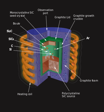
The Lely method produces bulk silicon carbide crystals through the process of sublimation. Silicon carbide powder is loaded into a graphite crucible, which is purged with Argon gas and heated to approximately 2,500 °C (4,530 °F). The silicon carbide near the outer walls of the crucible sublimes and is deposited on a graphite rod near the center of the crucible, which is at a lower temperature.[2]
Several modified versions of the Lely method exist, most commonly the silicon carbide is heated from the bottom end rather than the walls of the crucible, and deposited on the lid. Other modifications include varying the temperature, temperature gradient, Argon pressure, and geometry of the system. Typically, an induction furnace is used to achieve the required temperatures of 1,800–2,600 °C (3,270–4,710 °F).[2]:195
See also
- Acheson process
- Czochralski process
- Sublimation sandwich method
References
- US2854364 (A), Lely, Jan Anthony, "Sublimation process for manufacturing silicon carbide crystals", published 7 March 1955, issued 30 September 1958
- Byrappa, Kullaiah; Ohachi, Tadashi (2003). Crystal Growth Technology. Springer Science & Business Media. ISBN 9783540003670. Retrieved 10 September 2018.