LIGA
LIGA is a German acronym for Lithographie, Galvanoformung, Abformung (Lithography, Electroplating, and Molding) that describes a fabrication technology used to create high-aspect-ratio microstructures.
Overview
The LIGA consists of three main processing steps; lithography, electroplating and molding. There are two main LIGA-fabrication technologies, X-Ray LIGA, which uses X-rays produced by a synchrotron to create high-aspect ratio structures, and UV LIGA, a more accessible method which uses ultraviolet light to create structures with relatively low aspect ratios.
The notable characteristics of X-ray LIGA-fabricated structures include:
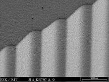
- high aspect ratios on the order of 100:1
- parallel side walls with a flank angle on the order of 89.95°
- smooth side walls with = 10 nm, suitable for optical mirrors
- structural heights from tens of micrometers to several millimeters
- structural details on the order of micrometers over distances of centimeters
X-Ray LIGA
X-Ray LIGA is a fabrication process in microtechnology that was developed in the early 1980s [1] by a team under the leadership of Erwin Willy Becker and Wolfgang Ehrfeld at the Institute for Nuclear Process Engineering (Institut für Kernverfahrenstechnik, IKVT) at the Karlsruhe Nuclear Research Center, since renamed to the Institute for Microstructure Technology (Institut für Mikrostrukturtechnik, IMT) at the Karlsruhe Institute of Technology (KIT). LIGA was one of the first major techniques to allow on-demand manufacturing of high-aspect-ratio structures (structures that are much taller than wide) with lateral precision below one micrometer.
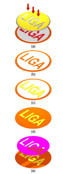
In the process, an X-ray sensitive polymer photoresist, typically PMMA, bonded to an electrically conductive substrate, is exposed to parallel beams of high-energy X-rays from a synchrotron radiation source through a mask partly covered with a strong X-ray absorbing material. Chemical removal of exposed (or unexposed) photoresist results in a three-dimensional structure, which can be filled by the electrodeposition of metal. The resist is chemically stripped away to produce a metallic mold insert. The mold insert can be used to produce parts in polymers or ceramics through injection molding.
The LIGA technique's unique value is the precision obtained by the use of deep X-ray lithography (DXRL). The technique enables microstructures with high aspect ratios and high precision to be fabricated in a variety of materials (metals, plastics, and ceramics). Many of its practitioners and users are associated with or are located close to synchrotron facilities.
UV LIGA
UV LIGA utilizes an inexpensive ultraviolet light source, like a mercury lamp, to expose a polymer photoresist, typically SU-8. Because heating and transmittance are not an issue in optical masks, a simple chromium mask can be substituted for the technically sophisticated X-ray mask. These reductions in complexity make UV LIGA much cheaper and more accessible than its X-ray counterpart. However, UV LIGA is not as effective at producing precision molds and is thus used when cost must be kept low and very high aspect ratios are not required.
Process details
Mask
X-ray masks are composed of a transparent, low-Z carrier, a patterned high-Z absorber, and a metallic ring for alignment and heat removal. Due to extreme temperature variations induced by the X-ray exposure, carriers are fabricated from materials with high thermal conductivity to reduce thermal gradients. Currently, vitreous carbon and graphite are considered the best material, as their use significantly reduces side-wall roughness. Silicon, silicon nitride, titanium, and diamond are also in use as carrier substrates but not preferred, as the required thin membranes are comparatively fragile and titanium masks tend to round sharp features due to edge fluorescence. Absorbers are gold, nickel, copper, tin, lead, and other X-ray absorbing metals.
Masks can be fabricated in several fashions. The most accurate and expensive masks are those created by electron beam lithography, which provides resolutions as fine as 0.1 µm in resist 4 µm thick and 3 µm features in resist 20 µm thick. An intermediate method is the plated photomask which provides 3 µm resolution and can be outsourced at a cost on the order of $1000 per mask. The least expensive method is a direct photomask, which provides 15 µm resolution in resist 80 µm thick. In summary, masks can cost between $1000 and $20,000 and take between two weeks and three months for delivery. Due to the small size of the market, each LIGA group typically has its own mask-making capability. Future trends in mask creation include larger formats, from a diameter of 100 mm to 150 mm, and smaller feature sizes.
Substrate
The starting material is a flat substrate, such as a silicon wafer or a polished disc of beryllium, copper, titanium, or other material. The substrate, if not already electrically conductive, is covered with a conductive plating base, typically through sputtering or evaporation.
The fabrication of high-aspect-ratio structures requires the use of a photoresist able to form a mold with vertical sidewalls. Thus the photoresist must have a high selectivity and be relatively free from stress when applied in thick layers. The typical choice, poly(methyl methacrylate) (PMMA) is applied to the substrate by a glue-down process in which a precast, high-molecular-weight sheet of PMMA is attached to the plating base on the substrate. The applied photoresist is then milled down to the precise height by a fly cutter prior to pattern transfer by X-ray exposure. Because the layer must be relatively free from stress, this glue-down process is preferred over alternative methods such as casting. Further, the cutting of the PMMA sheet by the fly cutter requires specific operating conditions and tools to avoid introducing any stress and crazing of the photoresist.
Exposure
A key enabling technology of LIGA is the synchrotron, capable of emitting high-power, highly collimated X-rays. This high collimation permits relatively large distances between the mask and the substrate without the penumbral blurring that occurs from other X-ray sources. In the electron storage ring or synchrotron, a magnetic field constrains electrons to follow a circular path and the radial acceleration of the electrons causes electromagnetic radiation to be emitted forward. The radiation is thus strongly collimated in the forward direction and can be assumed to be parallel for lithographic purposes. Because of the much higher flux of usable collimated X-rays, shorter exposure times become possible. Photon energies for a LIGA exposure are approximately distributed between 2.5 and 15 keV.
Unlike optical lithography, there are multiple exposure limits, identified as the top dose, bottom dose, and critical dose, whose values must be determined experimentally for a proper exposure. The exposure must be sufficient to meet the requirements of the bottom dose, the exposure under which a photoresist residue will remain, and the top dose, the exposure over which the photoresist will foam. The critical dose is the exposure at which unexposed resist begins to be attacked. Due to the insensitivity of PMMA, a typical exposure time for a 500 µm thick PMMA is six hours. During exposure, secondary radiation effects such as Fresnel diffraction, mask and substrate fluorescence, and the generation of Auger electrons and photoelectrons can lead to overexposure.
During exposure the X-ray mask and the mask holder are heated directly by X-ray absorption and cooled by forced convection from nitrogen jets. Temperature rise in PMMA resist is mainly from heat conducted from the substrate backward into the resist and from the mask plate through the inner cavity air forward to the resist, with X-ray absorption being tertiary. Thermal effects include chemistry variations due to resist heating and geometry-dependent mask deformation.
Development
For high-aspect-ratio structures the resist-developer system is required to have a ratio of dissolution rates in the exposed and unexposed areas of 1000:1. The standard, empirically optimized developer is a mixture of tetrahydro-1,4-oxazine (20 %), 2-aminoethanol-1 (5 %), 2-(2-butoxyethoxy)ethanol (60 %), and water (15 %). This developer provides the required ratio of dissolution rates and reduces stress-related cracking from swelling in comparison to conventional PMMA developers. After development, the substrate is rinsed with deionized water and dried either in a vacuum or by spinning. At this stage, the PMMA structures can be released as the final product (e.g., optical components) or can be used as molds for subsequent metal deposition.
Electroplating
In the electroplating step, nickel, copper, or gold is plated upward from the metalized substrate into the voids left by the removed photoresist. Taking place in an electrolytic cell, the current density, temperature, and solution are carefully controlled to ensure proper plating. In the case of nickel deposition from NiCl2 in a KCl solution, Ni is deposited on the cathode (metalized substrate) and Cl2 evolves at the anode. Difficulties associated with plating into PMMA molds include voids, where hydrogen bubbles nucleate on contaminates; chemical incompatibility, where the plating solution attacks the photoresist; and mechanical incompatibility, where film stress causes the plated layer to lose adhesion. These difficulties can be overcome through the empirical optimization of the plating chemistry and environment for a given layout.
Stripping
After exposure, development, and electroplating, the resist is stripped. One method for removing the remaining PMMA is to flood expose the substrate and use the developing solution to cleanly remove the resist. Alternatively, chemical solvents can be used. Stripping of a thick resist chemically is a lengthy process, taking two to three hours in acetone at room temperature. In multilayer structures, it is common practice to protect metal layers against corrosion by backfilling the structure with a polymer-based encapsulant. At this stage, metal structures can be left on the substrate (e.g., microwave circuitry) or released as the final product (e.g., gears).
Replication
After stripping, the released metallic components can be used for mass replication through standard means of replication such as stamping or injection molding.
Commercialization
In the 1990s, LIGA was a cutting-edge MEMS fabrication technology, resulting in the design of components showcasing the technique's unique versatility. Several companies that begin using the LIGA process later changed their business model (e.g., Steag microParts becoming Boehringer Ingelheim microParts, Mezzo Technologies). Currently, only two companies, HTmicro and microworks, continue their work in LIGA, benefiting from limitations of other competing fabrication technologies. UV LIGA, due to its lower production cost, is employed more broadly by several companies, such as Tecan, Temicon, and Mimotec in Switzerland, who supply the Swiss watch market with metal parts made of Nickel and Nickel-Phosphorus.
Gallery
Below is a gallery of LIGA-fabricated structures arranged by date.
 A nozzle for uranium enrichment.[1]
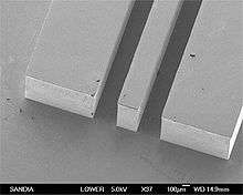 A 517 µm tall copper coplanar waveguide.[3]
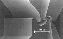
 Active part of a 2x2 optical switch, only the electrostatic actuator is shown.
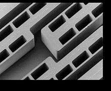
 Detail of the moulding tool for the LIGA microspectrometer.
 X-ray refractive x-ray lenses made of SU8 polymer. The patterns are made by tilting the mask and substrate in the beam twice by +-45°.
Notes
- Becker, E. W.; Ehrfeld, W.; Münchmeyer, D.; Betz, H.; Heuberger, A.; Pongratz, S.; Glashauser, W.; Michel, H. J.; Siemens, R. (1982). "Production of Separation-Nozzle Systems for Uranium Enrichment by a Combination of X-Ray Lithography and Galvanoplastics". Naturwissenschaften. 69 (11): 520–523. doi:10.1007/BF00463495.
- "Electroforming process". Retrieved 12 November 2018.
- Forman, Michael A. (2006). "Low-loss LIGA-fabricated coplanar waveguide and filter". 2006 Asia-Pacific Microwave Conference. pp. 1905–1907. doi:10.1109/APMC.2006.4429780. ISBN 978-4-902339-08-6.
See also
References
- Madou, M. (2003). Fundamentals of Microfabrication. CRC. ISBN 978-0849308260.
- Saile, V. (2009). LIGA and its Applications. Wiley-VCH. ISBN 978-3-527-31698-4.