Giant magnetoresistance
Giant magnetoresistance (GMR) is a quantum mechanical magnetoresistance effect observed in multilayers composed of alternating ferromagnetic and non-magnetic conductive layers. The 2007 Nobel Prize in Physics was awarded to Albert Fert and Peter Grünberg for the discovery of GMR.
The effect is observed as a significant change in the electrical resistance depending on whether the magnetization of adjacent ferromagnetic layers are in a parallel or an antiparallel alignment. The overall resistance is relatively low for parallel alignment and relatively high for antiparallel alignment. The magnetization direction can be controlled, for example, by applying an external magnetic field. The effect is based on the dependence of electron scattering on the spin orientation.
The main application of GMR is magnetic field sensors, which are used to read data in hard disk drives, biosensors, microelectromechanical systems (MEMS) and other devices.[1] GMR multilayer structures are also used in magnetoresistive random-access memory (MRAM) as cells that store one bit of information.
In literature, the term giant magnetoresistance is sometimes confused with colossal magnetoresistance of ferromagnetic and antiferromagnetic semiconductors, which is not related to the multilayer structure.[2][3]
Formulation
Magnetoresistance is the dependence of the electrical resistance of a sample on the strength of an external magnetic field. Numerically, it is characterized by the value
where R(H) is the resistance of the sample in a magnetic field H, and R(0) corresponds to H = 0.[4] Alternative forms of this expression may use electrical resistivity instead of resistance, a different sign for δH,[5] and are sometimes normalized by R(H) rather than R(0).[6]
The term "giant magnetoresistance" indicates that the value δH for multilayer structures significantly exceeds the anisotropic magnetoresistance, which has a typical value within a few percent.[7][8]
History
GMR was discovered in 1988 independently[9][10] by the groups of Albert Fert of the University of Paris-Sud, France, and Peter Grünberg of Forschungszentrum Jülich, Germany. The practical significance of this experimental discovery was recognized by the Nobel Prize in Physics awarded to Fert and Grünberg in 2007.[11]
Early steps
The first mathematical model describing the effect of magnetization on the mobility of charge carriers in solids, related to the spin of those carriers, was reported in 1936. Experimental evidence of the potential enhancement of δH has been known since the 1960s. By the late 1980s, the anisotropic magnetoresistance had been well explored,[12][13] but the corresponding value of δH did not exceed a few percent.[7] The enhancement of δH became possible with the advent of sample preparation techniques such as molecular beam epitaxy, which allows manufacturing multilayer thin films with a thickness of several nanometers.[14]
Experiment and its interpretation
Fert and Grünberg studied electrical resistance of structures incorporating ferromagnetic and non-ferromagnetic materials. In particular, Fert worked on multilayer films, and Grünberg in 1986 discovered the antiferromagnetic exchange interaction in Fe/Cr films.[14]
The GMR discovery work was carried out by the two groups on slightly different samples. The Fert group used (001)Fe/(001) Cr superlattices wherein the Fe and Cr layers were deposited in a high vacuum on a (001) GaAs substrate kept at 20 °C and the magnetoresistance measurements were taken at low temperature (typically 4.2 K).[10] The Grünberg work was performed on multilayers of Fe and Cr on (110) GaAs at room temperature.[9]
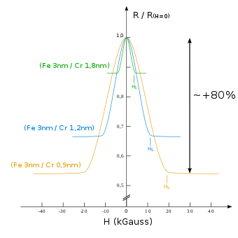
In Fe/Cr multilayers with 3-nm-thick iron layers, increasing the thickness of the non-magnetic Cr layers from 0.9 to 3 nm weakened the antiferromagnetic coupling between the Fe layers and reduced the demagnetization field, which also decreased when the sample was heated from 4.2 K to room temperature. Changing the thickness of the non-magnetic layers led to a significant reduction of the residual magnetization in the hysteresis loop. Electrical resistance changed by up to 50% with the external magnetic field at 4.2 K. Fert named the new effect giant magnetoresistance, to highlight its difference with the anisotropic magnetoresistance.[10][15] The Grünberg experiment[9] made the same discovery but the effect was less pronounced (3% compared to 50%) due to the samples being at room temperature rather than low temperature.
The discoverers suggested that the effect is based on spin-dependent scattering of electrons in the superlattice, particularly on the dependence of resistance of the layers on the relative orientations of magnetization and electron spins.[9][10] The theory of GMR for different directions of the current was developed in the next few years. In 1989, Camley and Barnaś calculated the "current in plane" (CIP) geometry, where the current flows along the layers, in the classical approximation,[16] whereas Levy et al. used the quantum formalism.[17] The theory of the GMR for the current perpendicular to the layers (current perpendicular to the plane or CPP geometry), known as the Valet-Fert theory, was reported in 1993.[18] Applications favor the CPP geometry[19] because it provides a greater magnetoresistance ratio (δH),[20] thus resulting in a greater device sensitivity.[21]
Theory
Fundamentals
Spin-dependent scattering
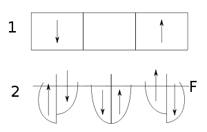
In magnetically ordered materials, the electrical resistance is crucially affected by scattering of electrons on the magnetic sublattice of the crystal, which is formed by crystallographically equivalent atoms with nonzero magnetic moments. Scattering depends on the relative orientations of the electron spins and those magnetic moments: it is weakest when they are parallel and strongest when they are antiparallel; it is relatively strong in the paramagnetic state, in which the magnetic moments of the atoms have random orientations.[7][22]
For good conductors such as gold or copper, the Fermi level lies within the sp band, and the d band is completely filled. In ferromagnets, the dependence of electron-atom scattering on the orientation of their magnetic moments is related to the filling of the band responsible for the magnetic properties of the metal, e.g., 3d band for iron, nickel or cobalt. The d band of ferromagnets is split, as it contains a different number of electrons with spins directed up and down. Therefore, the density of electronic states at the Fermi level is also different for spins pointing in opposite directions. The Fermi level for majority-spin electrons is located within the sp band, and their transport is similar in ferromagnets and non-magnetic metals. For minority-spin electrons the sp and d bands are hybridized, and the Fermi level lies within the d band. The hybridized spd band has a high density of states, which results in stronger scattering and thus shorter mean free path λ for minority-spin than majority-spin electrons. In cobalt-doped nickel, the ratio λ↑/λ↓ can reach 20.[23]
According to the Drude theory, the conductivity is proportional to λ, which ranges from several to several tens of nanometers in thin metal films. Electrons "remember" the direction of spin within the so-called spin relaxation length (or spin diffusion length), which can significantly exceed the mean free path. Spin-dependent transport refers to the dependence of electrical conductivity on the spin direction of the charge carriers. In ferromagnets, it occurs due to electron transitions between the unsplit 4s and split 3d bands.[7]
In some materials, the interaction between electrons and atoms is the weakest when their magnetic moments are antiparallel rather than parallel. A combination of both types of materials can result in a so-called inverse GMR effect.[7][24]
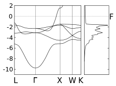 Copper (non-magnetic metal). F – the Fermi level. The vertical axis is energy in eV.
 Cobalt (majority spins)
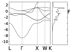 Cobalt (minority spins)
CIP and CPP geometries
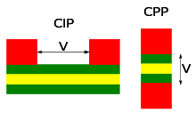
Electric current can be passed through magnetic superlattices in two ways. In the current in plane (CIP) geometry, the current flows along the layers, and the electrodes are located on one side of the structure. In the current perpendicular to plane (CPP) configuration, the current is passed perpendicular to the layers, and the electrodes are located on different sides of the superlattice.[7] The CPP geometry results in more than twice higher GMR, but is more difficult to realize in practice than the CIP configuration.[25][26]
Carrier transport through a magnetic superlattice
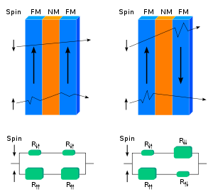
Magnetic ordering differs in superlattices with ferromagnetic and antiferromagnetic interaction between the layers. In the former case, the magnetization directions are the same in different ferromagnetic layers in the absence of applied magnetic field, whereas in the latter case, opposite directions alternate in the multilayer. Electrons traveling through the ferromagnetic superlattice interact with it much weaker when their spin directions are opposite to the magnetization of the lattice than when they are parallel to it. Such anisotropy is not observed for the antiferromagnetic superlattice; as a result, it scatters electrons stronger than the ferromagnetic superlattice and exhibits a higher electrical resistance.[7]
Applications of the GMR effect require dynamic switching between the parallel and antiparallel magnetization of the layers in a superlattice. In first approximation, the energy density of the interaction between two ferromagnetic layers separated by a non-magnetic layer is proportional to the scalar product of their magnetizations:
The coefficient J is an oscillatory function of the thickness of the non-magnetic layer ds; therefore J can change its magnitude and sign. If the ds value corresponds to the antiparallel state then an external field can switch the superlattice from the antiparallel state (high resistance) to the parallel state (low resistance). The total resistance of the structure can be written as
where R0 is the resistance of ferromagnetic superlattice, ΔR is the GMR increment and θ is the angle between the magnetizations of adjacent layers.[25]
Mathematical description
The GMR phenomenon can be described using two spin-related conductivity channels corresponding to the conduction of electrons, for which the resistance is minimum or maximum. The relation between them is often defined in terms of the coefficient of the spin anisotropy β. This coefficient can be defined using the minimum and maximum of the specific electrical resistivity ρF± for the spin-polarized current in the form
where ρF is the average resistivity of the ferromagnet.[27]
Resistor model for CIP and CPP structures
If scattering of charge carriers at the interface between the ferromagnetic and non-magnetic metal is small, and the direction of the electron spins persists long enough, it is convenient to consider a model in which the total resistance of the sample is a combination of the resistances of the magnetic and non-magnetic layers.
In this model, there are two conduction channels for electrons with various spin directions relative to the magnetization of the layers. Therefore, the equivalent circuit of the GMR structure consists of two parallel connections corresponding to each of the channels. In this case, the GMR can be expressed as
Here the subscript of R denote collinear and oppositely oriented magnetization in layers, χ = b/a is the thickness ratio of the magnetic and non-magnetic layers, and ρN is the resistivity of non-magnetic metal. This expression is applicable for both CIP and CPP structures. Under the condition this relationship can be simplified using the coefficient of the spin asymmetry
Such a device, with resistance depending on the orientation of electron spin, is called a spin valve. It is "open", if the magnetizations of its layers are parallel, and "closed" otherwise.[28]
Valet-Fert model
In 1993, Thierry Valet and Albert Fert presented a model for the giant magnetoresistance in the CPP geometry, based on the Boltzmann equations. In this model the chemical potential inside the magnetic layer is split into two functions, corresponding to electrons with spins parallel and antiparallel to the magnetization of the layer. If the non-magnetic layer is sufficiently thin then in the external field E0 the amendments to the electrochemical potential and the field inside the sample will take the form
where ℓs is the average length of spin relaxation, and the z coordinate is measured from the boundary between the magnetic and non-magnetic layers (z < 0 corresponds to the ferromagnetic).[18] Thus electrons with a larger chemical potential will accumulate at the boundary of the ferromagnet.[29] This can be represented by the potential of spin accumulation VAS or by the so-called interface resistance (inherent to the boundary between a ferromagnet and non-magnetic material)
where j is current density in the sample, ℓsN and ℓsF are the length of the spin relaxation in a non-magnetic and magnetic materials, respectively.[30]
Device preparation
Materials and experimental data
Many combinations of materials exhibit GMR,[31] and the most common are the following:
- FeCr[10]
- Co10Cu90: δH = 40% at room temperature[32]
- [110]Co95Fe5/Cu: δH = 110% at room temperature.[31]
The magnetoresistance depends on many parameters such as the geometry of the device (CIP or CPP), its temperature, and the thicknesses of ferromagnetic and non-magnetic layers. At a temperature of 4.2 K and a thickness of cobalt layers of 1.5 nm, increasing the thickness of copper layers dCu from 1 to 10 nm decreased δH from 80 to 10% in the CIP geometry. Meanwhile, in the CPP geometry the maximum of δH (125%) was observed for dCu = 2.5 nm, and increasing dCu to 10 nm reduced δH to 60% in an oscillating manner.[33]
When a Co(1.2 nm)/Cu(1.1 nm) superlattice was heated from near zero to 300 K, its δH decreased from 40 to 20% in the CIP geometry, and from 100 to 55% in the CPP geometry.[34]
The non-magnetic layers can be non-metallic. For example, δH up to 40% was demonstrated for organic layers at 11 K.[35] Graphene spin valves of various designs exhibited δH of about 12% at 7 K and 10% at 300 K, far below the theoretical limit of 109%.[36]
The GMR effect can be enhanced by spin filters that select electrons with a certain spin orientation; they are made of metals such as cobalt. For a filter of thickness t the change in conductivity ΔG can be expressed as
where ΔGSV is change in the conductivity of the spin valve without the filter, ΔGf is the maximum increase in conductivity with the filter, and β is a parameter of the filter material.[37]
Types of GMR
GMR is often classed by the type of devices which exhibit the effect.[38]
Films
Antiferromagnetic superlattices
GMR in films was first observed by Fert and Grünberg in a study of superlattices composed of ferromagnetic and non-magnetic layers. The thickness of the non-magnetic layers was chosen such that the interaction between the layers was antiferromagnetic and the magnetization in adjacent magnetic layers was antiparallel. Then an external magnetic field could make the magnetization vectors parallel thereby affecting the electrical resistance of the structure.[10]
Magnetic layers in such structures interact through antiferromagnetic coupling, which results in the oscillating dependence of the GMR on the thickness of the non-magnetic layer. In the first magnetic field sensors using antiferromagnetic superlattices, the saturation field was very large, up to tens of thousands of oersteds, due to the strong antiferromagnetic interaction between their layers (made of chromium, iron or cobalt) and the strong anisotropy fields in them. Therefore, the sensitivity of the devices was very low. The use of permalloy for the magnetic and silver for the non-magnetic layers lowered the saturation field to tens of oersteds.[39]
Spin valves using exchange bias
In the most successful spin valves the GMR effect originates from exchange bias. They comprise a sensitive layer, "fixed" layer and an antiferromagnetic layer. The last layer freezes the magnetization direction in the "fixed" layer. The sensitive and antiferromagnetic layers are made thin to reduce the resistance of the structure. The valve reacts to the external magnetic field by changing the magnetization direction in the sensitive layer relatively to the "fixed" layer.[39]
The main difference of these spin valves from other multilayer GMR devices is the monotonic dependence of the amplitude of the effect on the thickness dN of the non-magnetic layers:
where δH0 is a normalization constant, λN is the mean free path of electrons in the non-magnetic material, d0 is effective thickness that includes interaction between layers.[38][40] The dependence on the thickness of the ferromagnetic layer can be given as:
The parameters have the same meaning as in the previous equation, but they now refer to the ferromagnetic layer.[31]
Non-interacting multilayers (pseudospin valves)
GMR can also be observed in the absence of antiferromagnetic coupling layers. In this case, the magnetoresistance results from the differences in the coercive forces (for example, it is smaller for permalloy than cobalt). In multilayers such as permalloy/Cu/Co/Cu the external magnetic field switches the direction of saturation magnetization to parallel in strong fields and to antiparallel in weak fields. Such systems exhibit a lower saturation field and a larger δH than superlattices with antiferromagnetic coupling.[39] A similar effect is observed in Co/Cu structures. The existence of these structures means that GMR does not require interlayer coupling, and can originate from a distribution of the magnetic moments that can be controlled by an external field.[41]
Inverse GMR effect
In the inverse GMR, the resistance is minimum for the antiparallel orientation of the magnetization in the layers. Inverse GMR is observed when the magnetic layers are composed of different materials, such as NiCr/Cu/Co/Cu. The resistivity for electrons with opposite spins can be written as ; it has different values, i.e. different coefficients β, for spin-up and spin-down electrons. If the NiCr layer is not too thin, its contribution may exceed that of the Co layer, resulting in inverse GMR.[24] Note that the GMR inversion depends on the sign of the product of the coefficients β in adjacent ferromagnetic layers, but not on the signs of individual coefficients.[34]
Inverse GMR is also observed if NiCr alloy is replaced by vanadium-doped nickel, but not for doping of nickel with iron, cobalt, manganese, gold or copper.[42]
GMR in granular structures
GMR in granular alloys of ferromagnetic and non-magnetic metals was discovered in 1992 and subsequently explained by the spin-dependent scattering of charge carriers at the surface and in the bulk of the grains. The grains form ferromagnetic clusters about 10 nm in diameter embedded in a non-magnetic metal, forming a kind of superlattice. A necessary condition for the GMR effect in such structures is poor mutual solubility in its components (e.g., cobalt and copper). Their properties strongly depend on the measurement and annealing temperature. They can also exhibit inverse GMR.[32][43]
Applications
Spin-valve sensors
General principle
One of the main applications of GMR materials is in magnetic field sensors, e.g., in hard disk drives[25] and biosensors,[31] as well as detectors of oscillations in MEMS.[31] A typical GMR-based sensor consists of seven layers:
- Silicon substrate,
- Binder layer,
- Sensing (non-fixed) layer,
- Non-magnetic layer,
- Fixed layer,
- Antiferromagnetic (Pinning) layer,
- Protective layer.
The binder and protective layers are often made of tantalum, and a typical non-magnetic material is copper. In the sensing layer, magnetization can be reoriented by the external magnetic field; it is typically made of NiFe or cobalt alloys. FeMn or NiMn can be used for the antiferromagnetic layer. The fixed layer is made of a magnetic material such as cobalt. Such a sensor has an asymmetric hysteresis loop owing to the presence of the magnetically hard, fixed layer.[44][45]
Spin valves may exhibit anisotropic magnetoresistance, which leads to an asymmetry in the sensitivity curve.[46]
Hard disk drives
In hard disk drives (HDDs), information is encoded using magnetic domains, and a change in the direction of their magnetization is associated with the logical level 1 while no change represents a logical 0. There are two recording methods: longitudinal and perpendicular.
In the longitudinal method, the magnetization is normal to the surface. A transition region (domain walls) is formed between domains, in which the magnetic field exits the material. If the domain wall is located at the interface of two north-pole domains then the field is directed outward, and for two south-pole domains it is directed inward. To read the direction of the magnetic field above the domain wall, the magnetization direction is fixed normal to the surface in the antiferromagnetic layer and parallel to the surface in the sensing layer. Changing the direction of the external magnetic field deflects the magnetization in the sensing layer. When the field tends to align the magnetizations in the sensing and fixed layers, the electrical resistance of the sensor decreases, and vice versa.[47]
Magnetic RAM
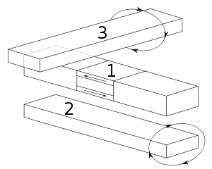
A cell of magnetoresistive random-access memory (MRAM) has a structure similar to the spin-valve sensor. The value of the stored bits can be encoded via the magnetization direction in the sensor layer; it is read by measuring the resistance of the structure. The advantages of this technology are independence of power supply (the information is preserved when the power is switched off owing to the potential barrier for reorienting the magnetization), low power consumption and high speed.[25]
In a typical GMR-based storage unit, a CIP structure is located between two wires oriented perpendicular to each other. These conductors are called lines of rows and columns. Pulses of electric current passing through the lines generate a vortex magnetic field, which affects the GMR structure. The field lines have ellipsoid shapes, and the field direction (clockwise or counterclockwise) is determined by the direction of the current in the line. In the GMR structure, the magnetization is oriented along the line.
The direction of the field produced by the line of the column is almost parallel to the magnetic moments, and it can not reorient them. Line of the row is perpendicular, and regardless of the magnitude of the field can rotate the magnetization by only 90 °. With the simultaneous passage of pulses along the row and column lines, of the total magnetic field at the location of the GMR structure will be directed at an acute angle with respect to one point and an obtuse to others. If the value of the field exceeds some critical value, the latter changes its direction.
There are several storage and reading methods for the described cell. In one method, the information is stored in the sensing layer; it is read via resistance measurement and is erased upon reading. In another scheme, the information is kept in the fixed layer, which requires higher recording currents compared to reading currents.[48]
Tunnel magnetoresistance (TMR) is an extension of spin-valve GMR, in which the electrons travel with their spins oriented perpendicularly to the layers across a thin insulating tunnel barrier (replacing the non-ferromagnetic spacer). This allows to achieve a larger impedance, a larger magnetoresistance value (~10x at room temperature) and a negligible temperature dependence. TMR has now replaced GMR in MRAMs and disk drives, in particular for high area densities and perpendicular recording.[49]
Other applications
Magnetoresistive insulators for contactless signal transmission between two electrically isolated parts of electrical circuits were first demonstrated in 1997 as an alternative to opto-isolators. A Wheatstone bridge of four identical GMR devices is insensitive to a uniform magnetic field and reacts only when the field directions are antiparallel in the neighboring arms of the bridge. Such devices were reported in 2003 and may be used as rectifiers with a linear frequency response.[31]
Notes
- This schematic does not include hysteresis because the shape of its loop in superlattices strongly depends on the thickness of non-magnetic layer d. Fert observed a clear hysteresis, with a saturation field of ~4 кG and a remanent magnetization of 60% of the saturation value, at dCu=1.8 nm. When dCu was reduced to 0.9 nm, the GMR reached a maximum, but the hysteresis loop collapsed; the saturation field increased to 20 kG, but the remanent field was very small. (Baibich et al. 1988)
Citations
- Reig, Cardoso & Mukhopadhyay 2013.
- Nagaev, E. L. (1996). "Lanthanum manganites and other giant-magnetoresistance magnetic conductors". Soviet Physics Uspekhi (in Russian). 166 (8): 833–858. doi:10.3367/UFNr.0166.199608b.0833.
- Raveau, B.; Rao, C. N. R., eds. (1998). Colossal Magnetoresistance, Charge Ordering and Related Properties of Manganese Oxides. World Scientific Publishing Co. p. 2. ISBN 978-981-02-3276-4.
- Hirota, E.; Inomata, K. (2002a). Giant Magneto-Resistance Devices. Springer. p. 30. ISBN 978-3-540-41819-1.
- Nikitin, S. A. (2004). "Гигантское магнитосопротивление" (PDF). Соросовский обозревательный журнал. 8 (2): 92–98.
- Pippard, Alfred Brian (2009). Magnetoresistance in Metals. Cambridge Studies in Low Temperature Physics. Volume 2. Cambridge University Press. p. 8. ISBN 978-052111880-4.
- Chappert, Claude; Fert, Albert; Nguyen Van Dau, Frédéric (2007). "The emergence of spin electronics in data storage". Nature Materials. 6 (11): 813–823. Bibcode:2007NatMa...6..813C. doi:10.1038/nmat2024. PMID 17972936.
- Hirota, E.; Inomata, K. (2002b). Giant Magneto-Resistance Devices. Springer. p. 23. ISBN 978-3-540-41819-1.
- Binasch, G.; Grunberg; Saurenbach; Zinn (1989). "Enhanced magnetoresistance in layered magnetic structures with antiferromagnetic interlayer exchange". Physical Review B. 39 (7): 4828–4830. Bibcode:1989PhRvB..39.4828B. doi:10.1103/PhysRevB.39.4828. PMID 9948867.
- Baibich et al. 1988.
- "The Nobel Prize in Physics 2007". Nobel Foundation. Archived from the original on 5 August 2011. Retrieved 27 February 2011.
- Seitz, Frederick; Turnbull, David (1957). Advances in Research and Applications. Solid State Physics. Volume 5. Academic Press. p. 31. ISBN 978-012607705-6.
- Aboaf, J. A. (9 October 1984). "New Magnetoresistive Materials". US Patent 4476454. Retrieved 11 April 2011.
- Fert, А. (2008a). "Nobel Lecture: Origin, development, and future of spintronics*". Rev. Mod. Phys. 80 (4): 1517–1530. Bibcode:2008RvMP...80.1517F. doi:10.1103/RevModPhys.80.1517. Fert, А. (2008b). "The origin, development and future of spintronics". Soviet Physics Uspekhi. 178 (12): 1336–1348. doi:10.3367/UFNr.0178.200812f.1336. (Reprints of the 2007 Nobel Lecture of 8 December 2007
- Tsymbal & Pettifor 2001, p. 120.
- Camley, R. E.; Barnaś, J. (1989). "Theory of giant magnetoresistance effects in magnetic layered structures with antiferromagnetic coupling". Phys. Rev. Lett. 63 (6): 664–667. Bibcode:1989PhRvL..63..664C. doi:10.1103/PhysRevLett.63.664. PMID 10041140.
- Fert, Albert; Levy, Peter M.; Zhang, Shufeng (1990). "Electrical conductivity of magnetic multilayered structures". Phys. Rev. Lett. 65 (13): 1643–1646. Bibcode:1990PhRvL..65.1643L. doi:10.1103/PhysRevLett.65.1643. PMID 10042322.
- Valet, T.; Fert, A. (1993). "Theory of the perpendicular magnetoresistance in magnetic multilayers". Physical Review B. 48 (10): 7099–7113. Bibcode:1993PhRvB..48.7099V. doi:10.1103/PhysRevB.48.7099.
- Nagasaka, K. (30 June 2005). "CPP-GMR Technology for Future High-Density Magnetic Recording" (PDF). Fujitsu. Archived from the original (PDF) on 6 August 2008. Retrieved 11 April 2011.
- Shinjo 2009.
- Buschow 2005, p. 580.
- Tsymbal & Pettifor 2001, p. 122.
- Tsymbal & Pettifor 2001, pp. 126–132.
- Buschow 2005, p. 254.
- Khvalkovskii, A.. V. "Гигантское магнитосопротивление: от открытия до Нобелевской премии". AMT&C. Archived from the original on 8 January 2015. Retrieved 27 February 2011.
- Bass, J.; Pratt, W. P. (1999b). "Current-perpendicular (CPP) magnetoresistance in magnetic metallic multilayers". Journal of Magnetism and Magnetic Materials. 200: 274–289. Bibcode:1999JMMM..200..274B. doi:10.1016/S0304-8853(99)00316-9.
- Tretyak, Lvov & Barabanov 2002, p. 243.
- Tretyak, Lvov & Barabanov 2002, pp. 258–261, 247–248.
- Stöhr, J.; Siegmann, H. C. (2006a). Magnetism: From Fundamentals to Nanoscale Dynamics. Springer-Verlag Berlin Heidelberg. p. 641. ISBN 978-354030282-7.
- Stöhr, J.; Siegmann, H. C. (2006b). Magnetism: From Fundamentals to Nanoscale Dynamics. Springer-Verlag Berlin Heidelberg. pp. 648–649. ISBN 978-354030282-7.
- Coehoorn, R. (2003). "Novel Magnetoelectronic Materials and Devices" (PDF). Giant magnetoresistance and magnetic interactions in exchange-biased spin-valves. Lecture Notes. Technische Universiteit Eindhoven. Archived from the original (PDF) on 24 July 2011. Retrieved 25 April 2011.
- Granovsky, A. B.; Ilyn, M.; Zhukov, A.; Zhukova, V.; Gonzalez, J. (2011). "Giant magnetoresistance of granular microwires: Spin-dependent scattering in integranular spacers" (PDF). Physics of the Solid State. 53 (2): 320–322. Bibcode:2011PhSS...53..320G. doi:10.1134/S1063783411020107.
- Buschow 2005, p. 248.
- Bass, J.; Pratt, W. P. (1999a). "Current-perpendicular (CPP) magnetoresistance in magnetic metallic multilayers". Journal of Magnetism and Magnetic Materials. 200: 274–289. Bibcode:1999JMMM..200..274B. doi:10.1016/S0304-8853(99)00316-9.
- Sun, Dali; Yin, L; Sun, C; Guo, H; Gai, Z; Zhang, X. G.; Ward, T. Z.; Cheng, Z; Shen, J (2010). "Giant Magnetoresistance in Organic Spin Valves". Physical Review Letters. 104 (23): 236602. Bibcode:2010PhRvL.104w6602S. doi:10.1103/PhysRevLett.104.236602. PMID 20867259.
- Qin, Rui; Lu, Jing; Lai, Lin; Zhou, Jing; Li, Hong; Liu, Qihang; Luo, Guangfu; Zhao, Lina; Gao, Zhengxiang; Mei, Wai Ning; Li, Guangping (2010). "Room-temperature giant magnetoresistance over one billion percent in a bare graphene nanoribbon device". Phys. Rev. B. 81 (23): 233403. Bibcode:2010PhRvB..81w3403Q. doi:10.1103/PhysRevB.81.233403.
- Bland, J. A. C.; Heinrich, B., eds. (2005). Ultrathin Magnetic Structures. Application of Nanomagnetism. IV. Springer. pp. 161–163. ISBN 978-3-540-21954-5.
- Tsymbal, Evgeny. "GMR Structures". University of Nebraska-Lincoln. Archived from the original on 12 December 2012. Retrieved 11 April 2011.
- Nalwa, Hari Singh (2002a). Handbook of thin film materials: Nanomaterials and magnetic thin films. Volume 5. Academic Press. pp. 518–519. ISBN 978-012512908-4.
- Nalwa, Hari Singh (2002b). Handbook of thin film materials: Nanomaterials and magnetic thin films. Volume 5. Academic Press. pp. 519, 525–526. ISBN 978-012512908-4.
- Pu, F. C. (1996). Shang, C. H.; Wang, Y. J. (eds.). Aspects of Modern Magnetism: Lecture Notes of the Eighth Chinese International Summer School of Physics Beijing, China 28 August-7 September, 1995. World Scientific. p. 122. ISBN 978-981022601-5.
- Guimarães, Alberto P. (2009). Principles of Nanomagnetism. Springer. p. 132. ISBN 978-3-642-01481-9.
- "Magnetic Domains in Granular GMR Materials". National Institute of Standards and Technology. Archived from the original on 12 August 2011. Retrieved 12 March 2011.
- Wormington, Matthew; Brown, Elliot (2001). An Investigation of Giant Magnetoresistance (GMR) Spinvalve Structures Using X-Ray Diffraction and Reflectivity (PDF). Advances in X-ray Analysis – proceedings of the Denver X-ray Conferences. Volume 44. The International Centre for Diffraction Data. pp. 290–294. Archived from the original (PDF) on 5 September 2014.
- Dodrill, B. C.; Kelley, B. J. "Magnetic In-line Metrology for GMR Spin-Valve Sensors" (PDF). Lake Shore Cryotronics. Archived from the original (PDF) on 5 January 2011. Retrieved 12 March 2011.
- Hartmann, U., ed. (2000). Magnetic Multilayers and Giant Magnetoresistance. Springer Series in Surface Sciences. Volume 37. Springer. p. 111. ISBN 978-3-540-65568-8.
- Tretyak, Lvov & Barabanov 2002, pp. 285–286.
- Tretyak, Lvov & Barabanov 2002, pp. 289–291.
- Zaitsev, D. D. "Магнетосопротивление, Туннельное". Словарь нанотехнологических и связанных с нанотехнологиями терминов. Роснано. Archived from the original on 23 December 2011. Retrieved 11 April 2011.
Bibliography
- Baibich, M. N.; Broto, J. M.; Fert, A.; Nguyen Van Dau, F.; Petroff, F.; Etienne, P.; Creuzet, G.; Friederich, A.; Chazelas, J. (1988). "Giant Magnetoresistance of (001)Fe/(001)Cr Magnetic Superlattices" (PDF). Physical Review Letters. 61 (21): 2472–2475. Bibcode:1988PhRvL..61.2472B. doi:10.1103/PhysRevLett.61.2472. PMID 10039127. Archived from the original (PDF) on 21 January 2014.
- Buschow, K. H. J. (2005). Concise encyclopedia of magnetic and superconducting materials (2nd ed.). Elsevier. ISBN 978-008044586-1.
- Reig, Candid; Cardoso, Susana; Mukhopadhyay, Subhas Chandra (2013). Giant Magnetoresistance (GMR) Sensors - From Basis to State-of-the-Art Applications. Springer. doi:10.1007/978-3-642-37172-1. ISBN 978-3-642-37171-4.
- Shinjo, Teruya (29 June 2009). Nanomagnetism and Spintronics. Elsevier. ISBN 978-008093216-3.
- Tretyak, O. V.; Lvov, V. A.; Barabanov, O. V. (2002). Фізичні основи спінової електроніки [Physical foundations of spin electronics] (in Ukrainian). Kiev University. ISBN 966-594-323-5.
- Tsymbal, E. Y.; Pettifor, D. G. (2001). "Perspectives of Giant Magnetoresistance". In Spaepen, Frans; Seitz, Frederick; Turnbull, David; Ehrenreich, Henry (eds.). Solid state physics. Solid State Physics: Advances in Research and Applications. Volume 56. Academic Press. ISBN 978-012607756-8.
External links
- Giant Magnetoresistance: The Really Big Idea Behind a Very Tiny Tool National High Magnetic Field Laboratory
- Presentation of GMR-technique (IBM Research)