Floorplan (microelectronics)
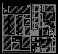
In electronic design automation, a floorplan of an integrated circuit is a schematics representation of tentative placement of its major functional blocks.

In modern electronic design process floorplans are created during the floorplanning design stage, an early stage in the hierarchical approach to integrated circuit design.
Depending on the design methodology being followed, the actual definition of a floorplan may differ.
Floorplanning
Floorplanning takes in some of the geometrical constraints in a design. Examples of this are:
- bonding pads for off-chip connections (often using wire bonding) are normally located at the circumference of the chip;
- line drivers often have to be located as close to bonding pads as possible;
- chip area is therefore in some cases given a minimum area in order to fit in the required number of pads;
- areas are clustered in order to limit data paths thus frequently featuring defined structures such as cache RAM, multiplier, barrel shifter, line driver and arithmetic logic unit;
- purchased intellectual property blocks (IP-blocks), such as a processor core, come in predefined area blocks;
- some IP-blocks come with legal limitations such as permitting no routing of signals directly above the block.
Mathematical models and optimization problems
In some approaches the floorplan may be a partition of the whole chip area into axis aligned rectangles to be occupied by IC blocks. This partition is subject to various constraints and requirements of optimization: block area, aspect ratios, estimated total measure of interconnects, etc.
Finding good floorplans has been a research area in combinatorial optimization. Most of the problems related to finding optimal floorplans are NP-hard, i.e., require vast computational resources. Therefore, the most common approach is to use various optimization heuristics for finding good solutions.
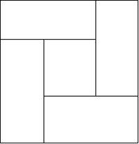
Another approach is to restrict design methodology to certain classes of floorplans, such as sliceable floorplans.
Sliceable floorplans


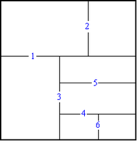
A sliceable floorplan is a floorplan that may be defined recursively as described below. [1]
- A floorplan that consists of a single rectangular block is sliceable.
- If a block from a sliceable floorplan is cut ("sliced") in two by a vertical or horizontal line, the resulting floorplan is sliceable.
Sliceable floorplans have been used in a number of early Electronic Design Automation tools[1] for a number of reasons. Sliceable floorplans may be conveniently represented by binary trees (more specifically, k-d trees), which correspond to the order of slicing. More importantly, a number of NP-hard problems with floorplans have polynomial time algorithms when restricted to sliceable floorplans.[2]
Further reading
References
- "The Electrical Engineering Handbook", Richard C. Dorf (1997) ISBN 0-8493-8574-1
- Sarrafzadeh, M, "Transforming an arbitrary floorplan into a sliceable one", Proc. 1993 IEEE/ACM International Conference on Computer-Aided Design (ICCAD-93), pp. 386-389.