Fan-out wafer-level packaging
Fan-out wafer-level packaging (also known as wafer-level fan-out packaging, fan-out WLP, FOWL packaging, FO-WLP, FOWLP, etc.) is an integrated circuit packaging technology, and an enhancement of standard wafer-level packaging (WLP) solutions.[1][2]

In conventional technologies, a wafer is diced first, and then individual dies are packaged; package size is usually considerably larger than the die size. By contrast, in standard WLP flows integrated circuits are packaged while still part of the wafer, and the wafer (with outer layers of packaging already attached) is diced afterwards; the resulting package is practically of the same size as the die itself. However, the advantage of having a small package comes with a downside of limiting the number of external contacts that can be accommodated in the limited package footprint; this may become a significant limitation when complex semiconductor devices requiring a large number of contacts are considered.
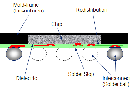
Fan-out WLP was developed to relax that limitation. It provides a smaller package footprint along with improved thermal and electrical performance compared to conventional packages, and allows having higher number of contacts without increasing the die size.
In contrast to standard WLP flows, in fan-out WLP the wafer is diced first. But then the dies are very precisely re-positioned on a carrier wafer or panel, with space for fan-out kept around each die. The carrier is then reconstituted by molding, followed by making redistribution layer atop the entire molded area (both atop the chip and atop the adjacent fan-out area), and then forming solder balls on top.
References
- Korczynski, Ed (May 5, 2014). "Wafer-level packaging of ICs for mobile systems of the future". Semiconductor Manufacturing & Design Community. Archived from the original on August 16, 2018. Retrieved September 24, 2018.
- "Fan-out Wafer Level Packaging". Orbotech. n.d. Archived from the original on September 22, 2018. Retrieved September 24, 2018.
External links
- "Fan-out Wafer Level Packaging (FOWLP)". 3dic.org. October 12, 2016. Archived from the original on September 23, 2018. Retrieved September 24, 2018.
- Butler, David (August 2016). "Fan-Out Wafer Level Packaging: Breakthrough advantages and surmountable challenges". Solid State Technology (www.solid-state.com). Archived from the original on September 24, 2018. Retrieved September 24, 2018.
- "Fan-Out Wafer Level Packaging. Patent Landscape Analysis" (PDF). Know Made Patent & Technology Intelligence. November 2016. Archived (PDF) from the original on September 24, 2018. Retrieved September 24, 2018.