Die preparation
Die preparation is a step of semiconductor device fabrication during which a wafer is prepared for IC packaging and IC testing. The process of die preparation typically consists of two steps: wafer mounting and wafer dicing.

Wafer mounting
Wafer mounting is a step that is performed during the die preparation of a wafer as part of the process of semiconductor fabrication. During this step, the wafer is mounted on a plastic tape that is attached to a ring. Wafer mounting is performed right before the wafer is cut into separate dies. The adhesive film upon which the wafer is mounted ensures that the individual dies remain firmly in place during 'dicing', as the process of cutting the wafer is called.
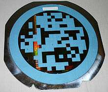
The picture on the right shows a 300 mm wafer after it was mounted and diced. The blue plastic is the adhesive tape. The wafer is the round disc in the middle. In this case, a large number of dies were already removed.
Semiconductor-die cutting
In the manufacturing of micro-electronic devices, die cutting, dicing or singulation is a process of reducing a wafer containing multiple identical integrated circuits to individual dies each containing one of those circuits.
During this process, a wafer with up to thousands of circuits is cut into rectangular pieces, each called a die. In between those functional parts of the circuits, a thin non-functional spacing is foreseen where a saw can safely cut the wafer without damaging the circuits. This spacing is called the scribe line or saw street. The width of the scribe is very small, typically around 100 μm. A very thin and accurate saw is therefore needed to cut the wafer into pieces. Usually the dicing is performed with a water-cooled circular saw with diamond-tipped teeth.
Types of blades
The most common make up of blade used is either a metal or resin bond containing abrasive grit of natural or more commonly synthetic diamond, or borazon in various forms. Alternatively, the bond and grit may be applied as a coating to a metal former. See diamond tools.
Further reading
- Kaeslin, Hubert (2008), Digital Integrated Circuit Design, from VLSI Architectures to CMOS Fabrication, Cambridge University Press, section 11.4.