Contact pad
Contact pads or bond pads are designated surface areas of a printed circuit board (PCB) or die of an integrated circuit. Possibilities to contact to pads include soldering, wirebonding, flip chip mounting, or probe needles.
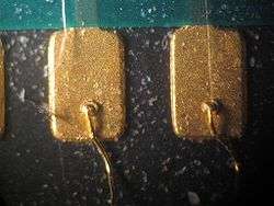
Gold wire ball-bonded to a gold contact pad
Further reading
- Jing Li, Evaluation and Improvement of the Robustness of a PCB Pad in a Lead-free Environment, ProQuest, 2007 ISBN 0-549-32110-1.
- Kraig Mitzner, Complete PCB Design Using OrCAD Capture and PCB Editor, Newnes, 2009 ISBN 0-08-094354-3.
- Deborah Lea, Fredirikus Jonck, Christopher Hunt, Solderability Measurements of PCB Pad Finishes and Geometries, National Physical Laboratory, 2001 OCLC 59500348.
gollark: You don't pick B, you pick either just A or A+B.
gollark: But, considering only somehow "real" universes, your choice after the boxes are filled can't affect the contents and it's "strictly better" to take both, as this provides more money than taking one. But everyone who does this gets less money than the oneboxer people due to them being predicted as doing that. Thus paradox.
gollark: The osmarks.tk™ superintelligent AI will be programmed to kill LyricLy and only LyricLy due to this.
gollark: I refuse to negotiate (acausally) with future terroristic AIs.
gollark: STOP INFOHAZARDING US.
This article is issued from Wikipedia. The text is licensed under Creative Commons - Attribution - Sharealike. Additional terms may apply for the media files.