Beam lead technology
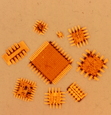
Beam lead technology is a method of fabricating a semiconductor device. Its original application was to high-frequency silicon switching transistors and high-speed integrated circuits. It eliminated the labor-intensive wire-bonding process used for integrated circuits at the time and allowed automated assembly of semiconductor chips onto larger substrates to produce hybrid integrated circuits. [1]

History
In the early 1960s, M.P. Lepselter[2][3] developed the techniques for fabricating a structure consisting of electroforming an array of thick, self-supporting gold patterns on a thin film Ti-Pt Au base, hence the name "beams", deposited on the surface of a silicon wafer. The excess semiconductor from under the beams was removed, thereby separating the individual devices and leaving them with self-supporting beam leads or internal chiplets cantilevered beyond the semiconductor. The contacts served as electrical leads in addition to also serving the purpose of structural support for the devices.
Patents
Patented inventions included:
- Selective Removal of Material Using Cathodic Sputtering (Plasma Etching/RIE), US Patent #3,271,286; issued 1966
- PtSi Semiconductor Contacts and Schottky Diodes (PtSi Schottky Diodes), US Patent #3,274,670; issued 1966
- Semiconductive Device Including Beam Leads (Beam Leads, Ti-Pt-Au metal system), US Patent #3,426,252; issued 1969
- Method for Making Closely Spaced Conductive Layers (Air-Insulated Crossovers, air bridges, RF-Switch), US Patent #3,461,524; issued 1969
- Vibratory Reed Device (MEMS), US Patent #3,609,593; issued 1971
Legacy
This technology, also known as air-bridge technology, has established itself for its unsurpassed reliability in high-frequency silicon switching transistors and ultra-high-speed integrated circuits for telecommunications and missile systems. The beam lead devices, produced by the hundreds of millions, became the first example of a commercial microelectromechanical structure (MEMS).
References
- Rao R. Tummala et al, Microelectronics Packaging Handbook: Semiconductor packaging, Springer, 1997 ISBN 0-412-08441-4, page 8-75
- M.P. Lepselter, et al., "Beam-Lead Devices and Integrated Circuits", Proceedings of the IEEE, Vol. 53 No 4 (1965), p.405.
- Presentation at Electron Devices Meeting, October 29, 1964, Washington, D.C.
- Beam Lead Technology, M.P.Lepselter, Bell System Technical Journal 45. (2) (1966), pp. 233–253