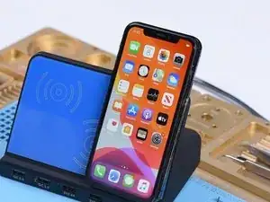
Introduction
-
-
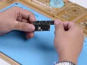
First of all, run a cosmetic inspection of the motherboard. The motherboard is not deformed or water-damaged.
-
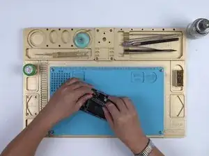
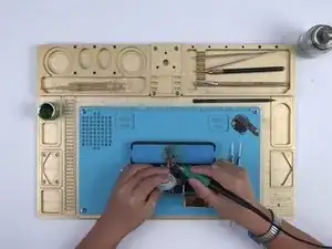
In the next place, assemble the phone and test.
-
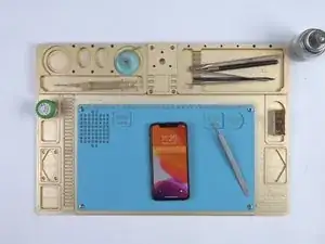
Press the power button to turn on the phone. The phone turns on normally.
-
-
-
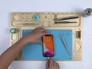
Plug in the charging cable. The phone can be charged with the charging cable.
-
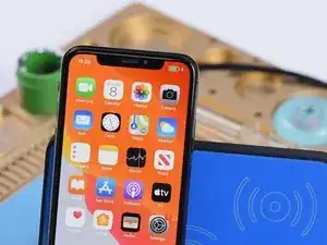
Place the phone on a wireless charger. The phone cannot be wirelessly charged..
-
We need to focus on wireless charging relevant circuits.
-
-
-
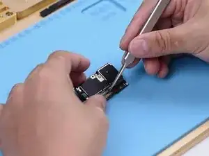
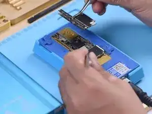
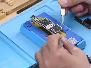
Take apart the phone and take out the motherboard. Remove the dust-proof sponge covering the board first.
-
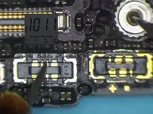
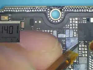
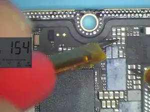
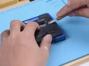
Then run diode mode measurement of the wireless charging connector. The measured value is normal, which indicates that wireless charging relevant circuits on the bonding pad are normal. We need to move on to wireless charging relevant circuits on the lower layer.
-
-
-
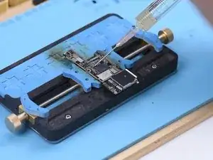
The first thing we do is to separate the upper layer from the lower layer. Place the motherboard on the heating platform and fit a screw into the screw hole on the motherboard. So we can take down the upper layer efficiently afterward.
-
Heat the motherboard for 2 minutes on the heating platform at 165℃.
-
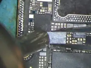
After heating, take down the upper layer with tweezers and then the lower layer.
-
-
-
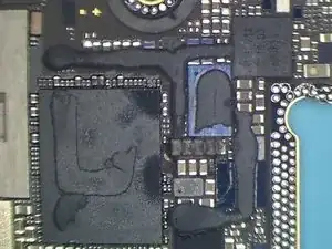
Run a cosmetic inspection of the lower layer. Nothing goes wrong.
-
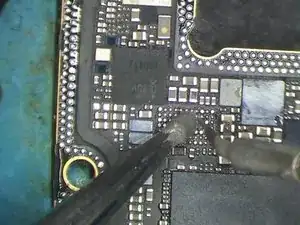
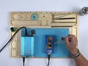
Run diode mode measurement of capacitors around the wireless charging IC. Judging by the measured value, there is no short-circuited condition.
-
Continue measuring diodes around the wireless charging IC. The measured value is also normal.
-
-
-
Let’s try to replace with a new wireless charging IC and see how it works.
-
Attach the lower layer to the PCB holder and apply some paste flux to the wireless charging IC.
-
Heat with QUICK 990 AD Hot Air Gun at 360℃, air flow 3 for about 1 minute. Take down the wireless charging IC from the board with tweezers.
-
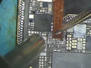
Continue to apply some medium-temp solder paste to the bonding pad. Heat with soldering iron at 365℃ to clean the bonding pad.
-
-
-
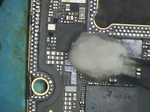
Once done, heat with Hot Air Gun at 360℃, air flow 3 to clean the bonding pad with rosin soaked solder wick.
-
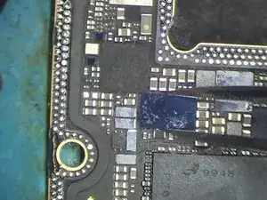
Clean with PCB cleaner afterward and apply some paste flux to the bonding pad.
-
-
-
Get a new wireless charging IC in the right position and solder with QUICK 990 AD Hot Air Gun at 360℃, air flow 3.
-
-
-
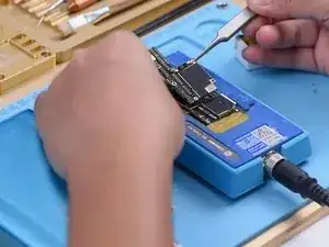
The next thing we need to do is to solder the two layers together. Clean the bonding pad before soldering.
-
Once done, get the bonding pad reballed.
-
-
-
Once completed, place the lower layer on the heating platform. Apply some BGA paste flux to the bonding pad and get the upper layer in the right position.
-
Heat for 2 minutes on the heating platform at 165℃.
-
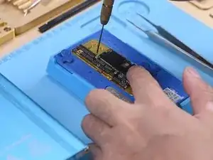
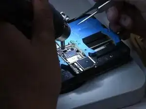
Now we can assemble the phone and test. Get the motherboard installed and display assembly connected. Press the power button to turn on the phone. The phone turns on normally.
-
Place the phone on a wireless charger and the phone can be wirelessly charged.
-

To reassemble your device, follow these instructions in reverse order.